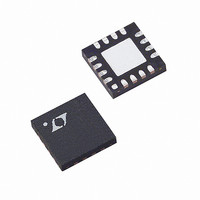
LT6402CUD-20#PBF Linear Technology, LT6402CUD-20#PBF Datasheet - Page 11

LT6402CUD-20#PBF
Manufacturer Part Number
LT6402CUD-20#PBF
Description
IC DIFF AMP/ADC DRVR 16-QFN
Manufacturer
Linear Technology
Datasheet
1.LT6402CUD-20PBF.pdf
(16 pages)
Specifications of LT6402CUD-20#PBF
Amplifier Type
Differential
Number Of Circuits
2
Output Type
Differential
Slew Rate
400 V/µs
-3db Bandwidth
300MHz
Current - Input Bias
5µA
Voltage - Input Offset
1000µV
Current - Supply
30mA
Current - Output / Channel
35mA
Voltage - Supply, Single/dual (±)
4 V ~ 5.5 V, ±2 V ~ 2.5 V
Operating Temperature
0°C ~ 70°C
Mounting Type
Surface Mount
Package / Case
16-WQFN Exposed Pad
No. Of Amplifiers
1
Input Offset Voltage
6.5mV
Gain Db Max
20dB
Bandwidth
300MHz
Supply Voltage Range
4V To 5.5V
Supply Current
30mA
Amplifier Case Style
QFN
Rohs Compliant
Yes
Lead Free Status / RoHS Status
Lead free / RoHS Compliant
Gain Bandwidth Product
-
Available stocks
Company
Part Number
Manufacturer
Quantity
Price
APPLICATIO S I FOR ATIO
Single-Ended to Differential Operation
The LT6402-20’s performance with single-ended inputs
is comparable to its performance with differential inputs.
This excellent single-ended performance is largely due
to the internal topology of the LT6402-20. Referring to
the block diagram, if the +INA and +INB pins are driven
with a single-ended signal (while –INA and –INB are tied
to AC ground), then the +OUT and –OUT pins are driven
differentially without any voltage swing needed from
amplifi er C. Single-ended to differential conversion using
more conventional topologies suffers from performance
limitations due to the common mode amplifi er.
Driving ADCs
The LT6402-20 has been specifi cally designed to interface
directly with high speed Analog to Digital Converters
(ADCs). In general, these ADCs have differential inputs, with
an input impedance of 1kΩ or higher. In addition, there is
generally some form of lowpass or bandpass fi ltering just
prior to the ADC to limit input noise at the ADC, thereby
improving system signal to noise ratio. Both the unfi ltered
Figure 3. Alternate Input Termination for Differential 50Ω
Input Impedance
IF IN
IF IN
Z
DIFFERENTIAL
IN
–
+
= 50Ω
U
100Ω
13
14
15
16
U
–INB
–INA
+INB
+INA
Figure 2. Input Termination for Differential 50Ω Input Impedance
LT6402-20
–OUT
+OUT
W
IF IN
IF IN
8
5
Z
DIFFERENTIAL
IN
–
+
= 50Ω
6402 F03
U
49.9Ω
49.9Ω
13
14
15
16
–INB
–INA
+INB
+INA
and fi ltered outputs of the LT6402-20 can easily drive the
high impedance inputs of these differential ADCs. If the
fi ltered outputs are used, then cutoff frequency and the
type of fi lter can be tailored for the specifi c application if
needed.
Wideband Applications
(Using the +OUT and –OUT Pins)
In applications where the full bandwidth of the LT6402-20
is desired, the unfi ltered output pins (+OUT and –OUT)
should be used. They have a low output impedance;
therefore, gain is unaffected by output load. Capacitance
in excess of 5pF placed directly on the unfi ltered outputs
results in additional peaking and reduced performance.
When driving an ADC directly, a small series resistance
is recommended between the LT6402-20’s outputs and
the ADC inputs (Figure 4). This resistance helps eliminate
any resonances associated with bond wire inductances of
either the ADC inputs or the LT6402-20’s outputs. A value
between 10Ω and 25Ω gives excellent results.
LT6402-20
–OUT
+OUT
Figure 4. Adding Small Series R at LT6402 Output
8
5
LT6402-20
–OUT
+OUT
6402 F02
8
5
10Ω TO 25Ω
10Ω TO 25Ω
LT6402-20
ADC
6402 F04
11
640220fa


