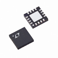
LTC6404CUD-1#PBF Linear Technology, LTC6404CUD-1#PBF Datasheet - Page 22

LTC6404CUD-1#PBF
Manufacturer Part Number
LTC6404CUD-1#PBF
Description
IC AMP/DRIVER DIFF 16-QFN
Manufacturer
Linear Technology
Type
ADC Driverr
Datasheet
1.LTC6404CUD-1PBF.pdf
(28 pages)
Specifications of LTC6404CUD-1#PBF
Applications
Data Acquisition
Mounting Type
Surface Mount
Package / Case
16-WQFN Exposed Pad
Current - Supply
27.8mA
Operating Temperature
0°C ~ 70°C
Output Type
Differential, Rail-to-Rail
Number Of Circuits
1
Current - Output / Channel
85mA
Amplifier Type
Differential
Voltage - Supply, Single/dual (±)
2.7 V ~ 5.5 V, ±1.35 V ~ 2.75 V
-3db Bandwidth
600MHz
Slew Rate
450 V/µs
Gain Bandwidth Product
500MHz
Current - Input Bias
23µA
Voltage - Input Offset
500µV
No. Of Amplifiers
1
Input Offset Voltage
2mV
Gain Db Max
1dB
Bandwidth
500MHz
Supply Voltage Range
2.7V To 5.25V
Supply Current
27.8mA
Amplifier Case Style
QFN
Rohs Compliant
Yes
Number Of Channels
1
Number Of Elements
1
Power Supply Requirement
Single
Common Mode Rejection Ratio
60dB
Voltage Gain Db
90dB
Unity Gain Bandwidth Product (typ)
500MHz
Input Resistance
1MOhm
Single Supply Voltage (typ)
3/5V
Dual Supply Voltage (typ)
Not RequiredV
Power Supply Rejection Ratio
60dB
Rail/rail I/o Type
Rail to Rail Output
Single Supply Voltage (min)
2.7V
Single Supply Voltage (max)
5.25V
Dual Supply Voltage (min)
Not RequiredV
Dual Supply Voltage (max)
Not RequiredV
Operating Temp Range
0C to 70C
Operating Temperature Classification
Commercial
Mounting
Surface Mount
Pin Count
16
Package Type
QFN EP
Lead Free Status / RoHS Status
Lead free / RoHS Compliant
Available stocks
Company
Part Number
Manufacturer
Quantity
Price
APPLICATIONS INFORMATION
LTC6404
According to Figure 4, the input impedance looking into
the differential amp (R
case, thus:
R2 is chosen to balance R1 || R
Input Common Mode Voltage Range
The LTC6404’s input common mode voltage (V
defi ned as the average of the two input voltages, V
V
input common mode range depends on the circuit con-
fi guration (gain), V
fully differential input applications, where V
the common mode input voltage is approximately:
22
IN
R
R
–
V
V
. It extends from V
ICM
INM
CM
2
=
•
=
R
=
R R
⎛
⎝ ⎜
I
I
V
⎛
⎜
⎝
R
+
•
IN
1
F
R
R
– •
+
+ +
S
S
F
2
+
1
2
R
I
V
⎞
⎠ ⎟
⎛
⎝ ⎜
IN
OCM
R
R
–
I
INM
I
R
V
≈
+
–
CM
V
V
and V
F
INM
to 1.4V below V
V
INP
R
) refl ects the single ended source
OCM
F
+
–
–
+
⎞
⎠ ⎟
⎞
⎟
⎠
CM
V
V
•
VOCM
0.01μF
SHDN
0.1μF
S
⎛
⎝ ⎜
V
V
:
(Refer to Figure 5). For
R
+
–
I
R
+
I
R
F
1
2
3
4
Figure 5. Circuit for Common Mode Range
+
SHDN
V
V
V
⎞
⎠ ⎟
. The operating
+
–
OCM
+
R
R
16
V
V
INP
5
I
I
SHDN
+
–
NC
NC
= –V
IN
ICM
15
6
+
, and
INM
IN
IN
) is
+
–
V
+
–
R
R
OCM
F
F
,
14
7
With singled ended inputs, there is an input signal com-
ponent to the input common mode voltage. Applying only
V
approximately:
Output Common Mode Voltage Range
The output common mode voltage is defi ned as the aver-
age of the two outputs:
The V
mode feedback loop which internally forces V
The output common mode range extends from 1.1V above
V
for the LTC6404-4 output common mode voltage range).
The V
sets the default mid-supply open circuit potential.
OUT
OUT
INP
–
to 1V below V
V
V
V
–
+
V
V
ICM
CM
OUTCM
(setting V
OUTF
OUTF
13
OCM
OCM
8
•
–
+
OUTF
OUTF
=
⎛
⎝ ⎜
V
pin sits in the middle of a voltage divider which
+
V
LTC6404
R
pin sets this average by an internal common
=
–
+
IN
V
V
F
–
–
R
6404 F05
V
+
+ +
F
V
V
V
V
INM
OCM
–
+
+
–
+
2
R
12
11
10
9
+
I
V
(see the Electrical Characteristics table
⎞
⎠ ⎟
IN
to zero), the input common voltage is
V
V
=
+
OUT
OUT
–
V
0.1μF
0.1μF
V
–
+
≈
OUT
INP
2
V
OCM
+
•
+
⎛
⎝ ⎜
2
0.1μF
0.1μF
0.1μF
R
V
•
V
V
V
OUT
⎛
⎝ ⎜
F
+
–
–
R
R
+
F
I
R
–
R
+
I
I
R
⎞
⎠ ⎟
F
⎞
⎠ ⎟
OUT
+
+
= –V
OUT
6404f
–
.


