LT1124CS8#PBF Linear Technology, LT1124CS8#PBF Datasheet - Page 10

LT1124CS8#PBF
Manufacturer Part Number
LT1124CS8#PBF
Description
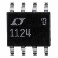
IC OP-AMP LOW NOISE DUAL 8-SOIC
Manufacturer
Linear Technology
Datasheet
1.LT1124CN8PBF.pdf
(18 pages)
Specifications of LT1124CS8#PBF
Amplifier Type
General Purpose
Number Of Circuits
2
Slew Rate
4.5 V/µs
Gain Bandwidth Product
12.5MHz
Current - Input Bias
8nA
Voltage - Input Offset
25µV
Current - Supply
2.3mA
Voltage - Supply, Single/dual (±)
±4 V ~ 18 V
Operating Temperature
0°C ~ 70°C
Mounting Type
Surface Mount
Package / Case
8-SOIC (3.9mm Width)
Lead Free Status / RoHS Status
Lead free / RoHS Compliant
Output Type
-
Current - Output / Channel
-
-3db Bandwidth
-
Available stocks
Company
Part Number
Manufacturer
Quantity
Price
APPLICATIONS INFORMATION
LT1124/LT1125
The LT1124 may be inserted directly into OP-270 sock-
ets. The LT1125 plugs into OP-470 sockets. Of course,
all standard dual and quad bipolar op amps can also be
replaced by these devices.
Matching Specifi cations
In many applications the performance of a system depends
on the matching between two op amps, rather than the
individual characteristics of the two devices. The three op
amp instrumentation amplifi er confi guration shown in this
data sheet is an example. Matching characteristics are not
100% tested on the LT1124/LT1125.
Some specifi cations are guaranteed by defi nition. For
example, 70μV maximum offset voltage implies that
mismatch cannot be more than 140μV. 112dB (= 2.5μV/V)
CMRR means that worst-case CMRR match is 106dB
Table 1. Expected Match
PARAMETER
V
Temperature Coeffi cient Match
Average Noninverting I
Match of Noninverting I
CMRR Match
PSRR Match
10
OS
Match, ΔV
OS
B
B
LT1124
LT1125
50% YIELD
0.35
126
127
20
30
6
7
Figure 1. Test Circuit for Offset Voltage and
Offset Voltage Drift with Temperature
LT1124AC/AM
LT1125AC/AM
*RESISTORS MUST HAVE LOW
100Ω*
50k*
THERMOELECTRIC POTENTIAL
V
OUT
= 1000V
–
+
98% YIELD
50k*
OS
110
150
115
118
1.0
–15V
18
22
15V
(5μV/V). However, Table 1 can be used to estimate the
expected matching performance between the two sides of
the LT1124, and between amplifi ers A and D, and between
amplifi ers B and C of the LT1125.
Offset Voltage and Drift
Thermocouple effects, caused by temperature gradients
across dissimilar metals at the contacts to the input
terminals, can exceed the inherent drift of the amplifi er
unless proper care is exercised. Air currents should be
minimized, package leads should be short, the two input
leads should be close together and maintained at the same
temperature.
The circuit shown in Figure 1 to measure offset voltage
is also used as the burn-in confi guration for the LT1124/
LT1125, with the supply voltages increased to ±16V.
1124/25 F01
V
OUT
50% YIELD
123
127
0.5
30
50
7
8
LT1124C/M
LT1125C/M
98% YIELD
130
180
112
114
1.5
25
30
UNITS
11245fe
μV/°C
nA
nA
dB
dB
μV
μV


