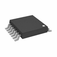
OP491GRUZ-REEL Analog Devices Inc, OP491GRUZ-REEL Datasheet - Page 17

OP491GRUZ-REEL
Manufacturer Part Number
OP491GRUZ-REEL
Description
IC OPAMP GP R-R 3MHZ 14TSSOP
Manufacturer
Analog Devices Inc
Datasheet
1.OP491GRUZ-REEL.pdf
(24 pages)
Specifications of OP491GRUZ-REEL
Slew Rate
0.5 V/µs
Amplifier Type
General Purpose
Number Of Circuits
4
Output Type
Rail-to-Rail
Gain Bandwidth Product
3MHz
Current - Input Bias
30nA
Voltage - Input Offset
80µV
Current - Supply
260µA
Current - Output / Channel
16mA
Voltage - Supply, Single/dual (±)
2.7 V ~ 12 V, ±1.35 V ~ 6 V
Operating Temperature
-40°C ~ 125°C
Mounting Type
Surface Mount
Package / Case
14-TSSOP
Op Amp Type
Low Power
No. Of Amplifiers
4
Bandwidth
3MHz
Supply Voltage Range
2.7V To 12V
Amplifier Case Style
TSSOP
No. Of Pins
14
Lead Free Status / RoHS Status
Lead free / RoHS Compliant
-3db Bandwidth
-
Lead Free Status / RoHS Status
Lead free / RoHS Compliant, Lead free / RoHS Compliant
Other names
OP491GRUZ-REEL
OP491GRUZ-REELTR
OP491GRUZ-REELTR
Available stocks
Company
Part Number
Manufacturer
Quantity
Price
Company:
Part Number:
OP491GRUZ-REEL
Manufacturer:
IR
Quantity:
1 500
Part Number:
OP491GRUZ-REEL
Manufacturer:
ADI/亚德诺
Quantity:
20 000
THEORY OF OPERATION
The OP191/OP291/OP491 are single-supply, micropower
amplifiers featuring rail-to-rail inputs and outputs. To achieve
wide input and output ranges, these amplifiers employ unique
input and output stages. In Figure 61 , the input stage comprises
two differential pairs, a PNP pair and an NPN pair. These two
stages do not work in parallel. Instead, only one stage is on for
any given input signal level. The PNP stage (Transistor Q1 and
Transistor Q2) is required to ensure that the amplifier remains
in the linear region when the input voltage approaches and
reaches the negative rail. On the other hand, the NPN stage
(Transistor Q5 and Transistor Q6) is needed for input voltages
up to and including the positive rail.
For the majority of the input common-mode range, the PNP
stage is active, as is shown in Figure 12. Notice that the bias
current switches direction at approximately 1.2 V to 1.3 V
below the positive rail. At voltages below this, the bias current
flows out of the OP291, indicating a PNP input stage. Above
this voltage, however, the bias current enters the device,
revealing the NPN stage. The actual mechanism within the
amplifier for switching between the input stages comprises
Transistor Q3, Transistor Q4, and Transistor Q7. As the input
common-mode voltage increases, the emitters of Q1 and Q2
follow that voltage plus a diode drop. Eventually, the emitters
of Q1 and Q2 are high enough to turn on Q3, which diverts the
8 μA of tail current away from the PNP input stage, turning it
off. Instead, the current is mirrored through Q4 and Q7 to
activate the NPN input stage.
+IN
5kΩ
Q1
Q2
8µA
Q4
Q3
5kΩ
–IN
Q5 Q6
Q7
Q8
Q9
Figure 61. Simplified Schematic
Rev. E | Page 17 of 24
Q10
Q11
Q12
Q13
Notice that the input stage includes 5 kΩ series resistors and
differential diodes, a common practice in bipolar amplifiers to
protect the input transistors from large differential voltages.
These diodes turn on whenever the differential voltage exceeds
approximately 0.6 V. In this condition, current flows between
the input pins, limited only by the two 5 kΩ resistors. This
characteristic is important in circuits where the amplifier may
be operated open-loop, such as a comparator. Evaluate each
circuit carefully to make sure that the increase in current does
not affect the performance.
The output stage in OP191 devices uses a PNP and an NPN
transistor, as do most output stages; however, Q32 and Q33, the
output transistors, are actually connected with their collectors
to the output pin to achieve the rail-to-rail output swing. As the
output voltage approaches either the positive or negative rail,
these transistors begin to saturate. Thus, the final limit on
output voltage is the saturation voltage of these transistors,
which is about 50 mV. The output stage does have inherent gain
arising from the collectors and any external load impedance.
Because of this, the open-loop gain of the amplifier is
dependent on the load resistance.
Q14
Q15
Q18
Q16
Q17
Q19
Q21
Q20
Q25
Q22
OP191/OP291/OP491
Q23
Q24
Q27
Q28
Q29
Q26
Q30
Q31
10pF
Q32
Q33
V
OUT


