LMC6464BIM/NOPB National Semiconductor, LMC6464BIM/NOPB Datasheet - Page 2

LMC6464BIM/NOPB
Manufacturer Part Number
LMC6464BIM/NOPB
Description
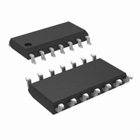
IC OP AMP QUAD MICPWR R-R 14SOIC
Manufacturer
National Semiconductor
Type
General Purpose Amplifierr
Datasheet
1.LMC6462AINNOPB.pdf
(20 pages)
Specifications of LMC6464BIM/NOPB
Amplifier Type
General Purpose
Number Of Circuits
4
Output Type
Rail-to-Rail
Slew Rate
0.028 V/µs
Gain Bandwidth Product
50kHz
Current - Input Bias
0.15pA
Voltage - Input Offset
250µV
Current - Supply
90µA
Current - Output / Channel
75mA
Voltage - Supply, Single/dual (±)
3 V ~ 15.5 V, ±1.5 V ~ 7.75 V
Operating Temperature
-40°C ~ 85°C
Mounting Type
Surface Mount
Package / Case
14-SOIC (3.9mm Width), 14-SOL
Rail/rail I/o Type
Rail to Rail Input/Output
Number Of Elements
4
Unity Gain Bandwidth Product
0.05MHz
Common Mode Rejection Ratio
65dB
Input Offset Voltage
3mV
Input Bias Current
150fA
Single Supply Voltage (typ)
5/9/12/15V
Dual Supply Voltage (typ)
Not RequiredV
Voltage Gain In Db
129.54dB
Power Supply Rejection Ratio
65dB
Power Supply Requirement
Single
Shut Down Feature
No
Single Supply Voltage (min)
3V
Single Supply Voltage (max)
15.5V
Dual Supply Voltage (min)
Not RequiredV
Dual Supply Voltage (max)
Not RequiredV
Technology
CMOS
Operating Temp Range
-40C to 85C
Operating Temperature Classification
Industrial
Mounting
Surface Mount
Pin Count
14
Package Type
SOIC N
Lead Free Status / RoHS Status
Lead free / RoHS Compliant
-3db Bandwidth
-
Lead Free Status / Rohs Status
Compliant
Other names
*LMC6464BIM
LMC6464BIM
LMC6464BIM
Available stocks
Company
Part Number
Manufacturer
Quantity
Price
Company:
Part Number:
LMC6464BIM/NOPB
Manufacturer:
TI/NSC
Quantity:
12 400
www.national.com
V
TCV
I
I
C
R
CMRR
+PSRR
−PSRR
V
Symbol
B
OS
OS
IN
IN
CM
Absolute Maximum Ratings
If Military/Aerospace specified devices are required,
please contact the National Semiconductor Sales Office/
Distributors for availability and specifications.
5V DC Electrical Characteristics
Unless otherwise specified, all limits guaranteed for T
limits apply at the temperature extremes.
ESD Tolerance (Note 2)
Differential Input Voltage
Voltage at Input/Output Pin
Supply Voltage (V
Current at Input Pin (Note 12)
Current at Output Pin
Current at Power Supply Pin
Lead Temp. (Soldering, 10 sec.)
Storage Temperature Range
Junction Temperature (Note 4)
OS
(Notes 3, 8)
Input Offset Voltage
Input Offset Voltage
Average Drift
Input Current
Input Offset Current
Common-Mode
Input Capacitance
Input Resistance
Common Mode
Rejection Ratio
Positive Power Supply
Rejection Ratio
Negative Power Supply
Rejection Ratio
Input Common-Mode
Voltage Range
Parameter
+
− V
−
)
(V
(Note 13)
(Note 13)
0V ≤ V
V
0V ≤ V
V
5V ≤ V
V
−5V ≤ V
V
V
For CMRR ≥ 50 dB
V
For CMRR ≥ 50 dB
+
+
−
+
+
+
+
) + 0.3V, (V
= 15V
= 5V
= 0V, V
= 0V, V
= 5V
= 15V
−65˚C to +150˚C
±
CM
CM
+
Conditions
−
Supply Voltage
≤ 15V,
≤ −15V,
≤ 15.0V,
≤ 5.0V
O
O
(Note 1)
= 2.5V
= −2.5V
−
) − 0.3V
±
±
30 mA
40 mA
2.0 kV
260˚C
150˚C
5 mA
J
16V
= 25˚C, V
2
(Note 5)
+
0.075
15.30
0.25
0.15
−0.2
5.30
−0.2
Typ
>
1.5
Operating Ratings
= 5V, V
85
85
85
85
3
Supply Voltage
Junction Temperature Range
Thermal Resistance (θ
Mount
10
LMC6462AM, LMC6464AM
LMC6462AI, LMC6464AI
LMC6462BI, LMC6464BI
N Package, 8-Pin Molded DIP
M Package, 8-Pin Surface
N Package, 14-Pin Molded DIP
M Package, 14-Pin
Surface Mount
−
LMC6462AI LMC6462BI
LMC6464AI LMC6464BI
= 0V, V
(Note 6)
−0.10
−0.15
15.25
15.00
Limit
0.00
5.25
5.00
0.00
0.5
1.2
10
70
67
70
67
70
67
70
67
5
CM
= V
JA
(Note 6)
O
)
−0.10
−0.15
Limit
15.25
15.00
0.00
5.25
5.00
0.00
= V
3.0
3.7
10
65
62
65
62
65
62
65
62
5
+
/2 and R
(Note 1)
LMC6462AM
LMC6464AM
−40˚C ≤ T
−40˚C ≤ T
(Note 6)
L
3.0V ≤ V
−0.10
−0.15
Limit
15.25
15.00
0.00
5.25
5.00
0.00
>
200
100
0.5
1.5
70
65
70
65
70
65
70
65
1M. Boldface
−55˚C ≤ T
J
J
+
115˚C/W
193˚C/W
126˚C/W
≤ +85˚C
≤ +85˚C
≤ 15.5V
81˚C/W
+125˚C
pA max
pA max
Tera Ω
Units
µV/˚C
max
max
max
min
min
min
min
min
mV
J
pF
dB
dB
dB
V
V
V
V
≤


