LMH6552SD/NOPB National Semiconductor, LMH6552SD/NOPB Datasheet - Page 19
LMH6552SD/NOPB
Manufacturer Part Number
LMH6552SD/NOPB
Description
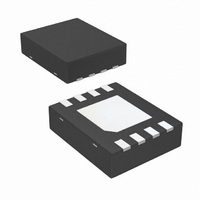
IC AMP DIFF 1.5GHZ 1CN 8-LLP
Manufacturer
National Semiconductor
Series
LMH®, PowerWise®r
Datasheet
1.LMH6552SDEVAL.pdf
(22 pages)
Specifications of LMH6552SD/NOPB
Amplifier Type
Differential
Number Of Circuits
1
Output Type
Differential
Slew Rate
3800 V/µs
-3db Bandwidth
1.5GHz
Current - Input Bias
60µA
Voltage - Input Offset
1500µV
Current - Supply
22.5mA
Current - Output / Channel
80mA
Voltage - Supply, Single/dual (±)
4.5 V ~ 12 V, ±2.25 V ~ 6 V
Operating Temperature
-40°C ~ 85°C
Mounting Type
Surface Mount
Package / Case
8-LLP
For Use With
LMH6552SDEVAL - BOARD EVALUATION FOR LMH6552
Lead Free Status / RoHS Status
Lead free / RoHS Compliant
Gain Bandwidth Product
-
Other names
LMH6552SD
LMH6552SD
LMH6552SDTR
LMH6552SD
LMH6552SDTR


for a given package (°C/W). For the SOIC package θ
150°C/W; LLP package θ
NOTE: If V
flowing in the feedback network. This current should be in-
cluded in the thermal calculations and added into the quies-
cent power dissipation of the amplifier.
THERMAL PERFORMANCE
The LLP package is designed for enhanced thermal perfor-
mance and features an exposed die attach pad (DAP) at the
bottom center of the package that creates a direct path to the
PCB for maximum power dissipation. The DAP is floating and
is not electrically connected to internal circuitry. Compared to
the traditional leaded packages where the die attach pad is
embedded inside the molding compound, the LLP reduces
one layer in the thermal path.
The thermal advantage of the LLP package is fully realized
only when the exposed die attach pad is soldered down to a
thermal land on the PCB board with thermal vias planted un-
derneath the thermal land. The thermal land can be connect-
ed to any power or ground plane within the allowable supply
voltage range of the device. Based on thermal analysis of the
LLP package, the junction-to-ambient thermal resistance
(θ
pad of the LLP package is soldered directly onto the PCB with
thermal land and thermal vias are 1.27 mm and 0.33 mm re-
spectively. Typical copper via barrel plating is 1 oz, although
thicker copper may be used to further improve thermal per-
formance.
For more information on board layout techniques, refer to Ap-
plication Note 1187 “Leadless Lead Frame Package (LLP).”
This application note also discusses package handling, sol-
der stencil and the assembly process.
ESD PROTECTION
The LMH6552 is protected against electrostatic discharge
(ESD) on all pins. The LMH6552 will survive 2000V Human
Body model and 200V Machine model events. Under normal
JA
) can be improved by a factor of two when the die attach
CM
is not 0V then there will be quiescent current
JA
is 58°C/W.
JA
is
19
operation the ESD diodes have no affect on circuit perfor-
mance. There are occasions, however, when the ESD diodes
will be evident. If the LMH6552 is driven by a large signal while
the device is powered down the ESD diodes will conduct . The
current that flows through the ESD diodes will either exit the
chip through the supply pins or will flow through the device,
hence it is possible to power up a chip with a large signal
applied to the input pins. Using the shutdown mode is one
way to conserve power and still prevent unexpected opera-
tion.
BOARD LAYOUT
The LMH6552 is a very high performance amplifier. In order
to get maximum benefit from the differential circuit architec-
ture board layout and component selection is very critical. The
circuit board should have a low inductance ground plane and
well bypassed broad supply lines. External components
should be leadless surface mount types. The feedback net-
work and output matching resistors should be composed of
short traces and precision resistors (0.1%). The output match-
ing resistors should be placed within 3 or 4 mm of the amplifier
as should the supply bypass capacitors. Refer to the section
titled Power Supply Bypassing for recommendations on by-
pass circuit layout. Evaluation boards are available free of
charge through the product folder on National’s web site.
By design, the LMH6552 is relatively insensitive to parasitic
capacitance at its inputs. Nonetheless, ground and power
plane metal should be removed from beneath the amplifier
and from beneath R
frequency.
With any differential signal path, symmetry is very important.
Even small amounts of asymmetry can contribute to distortion
and balance errors.
EVALUATION BOARD
See the LMH6552 Product Folder on www.national.com for
evaluation board availability and ordering information.
F
and R
G
for best performance at high
www.national.com
Related parts for LMH6552SD/NOPB
Image
Part Number
Description
Manufacturer
Datasheet
Request
R

Part Number:
Description:
Manufacturer:
National Semiconductor
Datasheet:
Part Number:
Description:
National Semiconductor [8-Bit D/A Converter]
Manufacturer:
National Semiconductor
Datasheet:
Part Number:
Description:
National Semiconductor [Media Coprocessor]
Manufacturer:
National Semiconductor
Datasheet:
Part Number:
Description:
Digitally Controlled Tone and Volume Circuit with Stereo Audio Power Amplifier, Microphone Preamp Stage and National 3D Sound
Manufacturer:
National Semiconductor
Datasheet:
Part Number:
Description:
Digitally Controlled Tone and Volume Circuit with Stereo Audio Power Amplifier, Microphone Preamp Stage and National 3D Sound
Manufacturer:
National Semiconductor
Datasheet:
Part Number:
Description:
AC97 Rev 2 Codec with Sample Rate Conversion and National 3D Sound
Manufacturer:
National Semiconductor
Part Number:
Description:
Manufacturer:
National Semiconductor
Datasheet:
Part Number:
Description:
Manufacturer:
National Semiconductor
Datasheet:
Part Number:
Description:
General Purpose, Low Voltage, Low Power, Rail-to-Rail Output Operational Amplifiers
Manufacturer:
National Semiconductor
Datasheet:
Part Number:
Description:
8-bit 20 MSPS flash A/D converter.
Manufacturer:
National Semiconductor
Datasheet:
Part Number:
Description:
Low Noise Quad Operational Amplifier
Manufacturer:
National Semiconductor
Datasheet:
Part Number:
Description:
Quad Differential Line Receivers
Manufacturer:
National Semiconductor
Datasheet:
Part Number:
Description:
Quad High Speed Trapezoidal? Bus Transceiver
Manufacturer:
National Semiconductor
Datasheet:
Part Number:
Description:
Dual Line Receiver
Manufacturer:
National Semiconductor
Datasheet: