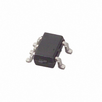
MAX4490AXK+T Maxim Integrated Products, MAX4490AXK+T Datasheet - Page 6

MAX4490AXK+T
Manufacturer Part Number
MAX4490AXK+T
Description
IC OP AMP SGL R-R I/O SC70-5
Manufacturer
Maxim Integrated Products
Datasheet
1.MAX4490AXKT.pdf
(8 pages)
Specifications of MAX4490AXK+T
Amplifier Type
General Purpose
Number Of Circuits
1
Output Type
Rail-to-Rail
Slew Rate
10 V/µs
Gain Bandwidth Product
10MHz
Current - Input Bias
50pA
Voltage - Input Offset
1500µV
Current - Supply
800µA
Current - Output / Channel
50mA
Voltage - Supply, Single/dual (±)
2.7 V ~ 5.5 V, ±1.35 V ~ 2.75 V
Operating Temperature
-40°C ~ 125°C
Mounting Type
Surface Mount
Package / Case
SC-70-5, SC-88A, SOT-323-5, SOT-353, 5-TSSOP
Number Of Channels
1
Voltage Gain Db
110 dB
Common Mode Rejection Ratio (min)
54 dB
Input Offset Voltage
10 mV
Operating Supply Voltage
3 V, 5 V
Supply Current
0.8 mA
Maximum Power Dissipation
200 mW
Maximum Operating Temperature
+ 125 C
Mounting Style
SMD/SMT
Maximum Dual Supply Voltage
+/- 2.75 V
Minimum Operating Temperature
- 40 C
Lead Free Status / RoHS Status
Lead free / RoHS Compliant
-3db Bandwidth
-
Lead Free Status / Rohs Status
Details
Other names
MAX4490AXK+T
MAX4490AXK+TTR
MAX4490AXK+TTR
pole at frequency (2πR′C
combination of the gain-setting resistors for the invert-
ing or noninverting amplifier configuration (Figure 2). If
the pole frequency is less than or comparable to the
unity-gain bandwidth (10MHz), the phase margin will
be reduced, and the amplifier will exhibit degraded
AC performance through either ringing in the step
response or sustained oscillations. The pole frequency is
10MHz when R′ = 3.2kΩ. To maximize stability, R′ <3kΩ
is recommended.
Applications that require rail-to-rail operation with mini-
mal loading (for small V
typically require R′ values >3kΩ. To improve step
response under these conditions, connect a small
Low-Cost, High-Slew-Rate,
Rail-to-Rail I/O Op Amps in SC70
Figure 1a. Output Source Current vs. Temperature
Figure 1b. Output Sink Current vs. Temperature
6
_______________________________________________________________________________________
6
5
4
3
2
1
0
9
8
7
6
5
4
3
2
1
0
-40
-40
-25
-25
V
-10
-10
DD
V
DD
= 2.7V
5 20 35 50 65 80
5 20 35
= 2.7V
TEMPERATURE (°C)
TEMPERATURE (°C)
DD
IN
)
-1
- V
50
, where R′ is the parallel
V
V
V
OH
V
V
V
DD
DD
DD
DD
DD
DD
65
- V
- V
- V
- V
- V
- V
80
and V
OH
OH
OH
V
OH
OH
OH
DD
V
= 200mV
= 100mV
= 50mV
DD
95 110
95
= 200mV
= 100mV
= 50mV
= 5V
= 5V
110
OL
125
125
- V
SS
) will
capacitor C
Choose C
where R
ting resistor (Figure 2).
Figure 3 shows the step response for a noninverting
amplifier subject to R′ = 4kΩ with and without the C
feedback capacitor.
Figure 2. Inverting and Noninverting Amplifier with Feedback
Compensation
f
V
is the feedback resistor and R is the gain-set-
INVERTING
NONINVERTING
IN
f
as follows:
f
between the inverting input and output.
R
R
V
C
IN
f
= 5(R / R
MAX4490
MAX4490
C
R
R
C
f
f
f
f
f
) [pf]
R′ = R || R
R
R′ = R || R
R
f
C
f
C
f
f
= RC
= RC
IN
f
IN
f
V
V
OUT
OUT
f


