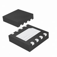
MAX4038ETA+T Maxim Integrated Products, MAX4038ETA+T Datasheet - Page 2

MAX4038ETA+T
Manufacturer Part Number
MAX4038ETA+T
Description
IC OP AMP R-R W/REF 8-TDFN
Manufacturer
Maxim Integrated Products
Datasheet
1.MAX4038ETAT.pdf
(22 pages)
Specifications of MAX4038ETA+T
Amplifier Type
General Purpose
Number Of Circuits
1
Output Type
Rail-to-Rail
Slew Rate
0.004 V/µs
Gain Bandwidth Product
4kHz
Current - Input Bias
1pA
Voltage - Input Offset
200µV
Current - Supply
1.9µA
Current - Output / Channel
13mA
Voltage - Supply, Single/dual (±)
1.4 V ~ 3.6 V
Operating Temperature
-40°C ~ 85°C
Mounting Type
Surface Mount
Package / Case
8-TDFN Exposed Pad
Number Of Channels
2
Voltage Gain Db
108 dB
Common Mode Rejection Ratio (min)
50 dB
Input Offset Voltage
2 mV
Operating Supply Voltage
3 V
Supply Current
0.0025 mA
Maximum Power Dissipation
1951 mW
Maximum Operating Temperature
+ 85 C
Mounting Style
SMD/SMT
Minimum Operating Temperature
- 40 C
Lead Free Status / RoHS Status
Lead free / RoHS Compliant
-3db Bandwidth
-
Lead Free Status / Rohs Status
Details
Other names
MAX4038ETA+T
MAX4038ETA+TTR
MAX4038ETA+TTR
ABSOLUTE MAXIMUM RATINGS
V
INA+, INB+, INA-, INB-, IN+, IN-, OUTA,
OUTA, OUTB, OUT, REF Shorted to V
Maximum Continuous Power Dissipation (T
Low I
with +1.2V Buffered Reference
Stresses beyond those listed under “Absolute Maximum Ratings” may cause permanent damage to the device. These are stress ratings only, and functional
operation of the device at these or any other conditions beyond those indicated in the operational sections of the specifications is not implied. Exposure to
absolute maximum rating conditions for extended periods may affect device reliability.
ELECTRICAL CHARACTERISTICS
(V
2
Supply Voltage Range
Supply Current
OPERATIONAL AMPLIFIERS
Input Offset Voltage
Input Bias Current
Input Offset Current
Input Common-Mode Voltage
Range
Common-Mode Rejection Ratio
Power-Supply Rejection Ratio
DD
DD
OUTB, OUT, REF .........................(V
5-Pin SC70 (derate 3.1mW/°C above +70°C) ..............247mW
6-Pin SOT23 (derate 8.7mW/°C above +70°C)............696mW
8-Pin µMAX (derate 4.5mW/°C above +70°C) .............362mW
8-Pin TDFN (derate 24.4mW/°C above +70°C) .........1951mW
_______________________________________________________________________________________
to V
= +3V, V
SS
PARAMETER
.............................................................-0.3V to +4.0V
SS
BIAS
= V
CM
= 0V, V
, +1.4V/800nA, Rail-to-Rail Op Amps
OUT_
= V
SS
SYMBOL
SS
CMRR
PSRR
V
V
V
or V
I
- 0.3V) to (V
DD
I
DD
OS
I
DD
CM
OS
B
A
/2, R
DD
= +70°C)
.......Continuous
L
MAX4036/MAX4038, guaranteed by PSRR
tests
MAX4037/MAX4039, guaranteed by PSRR
and line regulation tests
MAX4036
MAX4037
MAX4038
MAX4039
(Note 1)
(Note 1)
Guaranteed by
CMRR test
V
(MAX4036/MAX4038 only)
V
V
1.4V ≤ V
only)
1.8V ≤ V
to V
DD
DD
DD
DD
DD
= 1.4V, V
= 1.8V, V
= 3.3V, V
+ 0.3V)
/2, C
DD
DD
L
≤ 3.6V (MAX4036/MAX4038
≤ 3.6V
= 15pF, T
SS
SS
SS
CONDITIONS
≤ V
≤ V
≤ V
V
V
V
V
V
V
V
V
V
( M AX 4036/M AX 4038 onl y)
V
V
DD
DD
DD
DD
DD
DD
DD
DD
D D
DD
DD
Operating Temperature Range
Junction Temperature .....................................................+150°C
Storage Temperature Range .............................-65°C to +150°C
Lead Temperature (soldering, 10s) .................................+300°C
CM
CM
CM
9-Bump UCSP (derate 5.2mW/°C above +70°C).........412mW
10-Pin µMAX (derate 5.6mW/°C above +70°C) ...........444mW
10-Pin TDFN (derate 24.4mW/°C above +70°C) .......1951mW
MAX403_E_ _...................................................-40°C to +85°C
MAX403_A_ _ ................................................-40°C to +125°C
= 1.4V
= 1.4V
= 3.6V
= 1.8V
= 3.6V
= 1.4V
= 3.6V
= 1.8V
= 3.6V
= 1.8V
= 3.3V
A
≤ (V
≤ (V
≤ (V
= +25°C, unless otherwise specified.)
DD
DD
DD
- 0.4V)
- 0.3V)
- 0.2V)
V
V
V
MIN
50
50
56
62
62
1.4
1.8
SS
SS
SS
±0.2
±1.0
±0.3
TYP
70
70
76
82
84
0.8
0.9
1.9
2.0
1.7
1.9
2.8
3.0
V
V
V
±2.0
MAX
±10
±20
0.4
0.3
0.2
DD
DD
DD
3.6
3.6
1.2
1.3
2.4
2.5
2.3
2.5
4.0
4.1
-
-
-
UNITS
mV
pA
pA
dB
dB
µA
V
V


