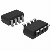
MAX4232AKA+T Maxim Integrated Products, MAX4232AKA+T Datasheet - Page 9

MAX4232AKA+T
Manufacturer Part Number
MAX4232AKA+T
Description
IC OP AMP R-R W/SD SOT23-8
Manufacturer
Maxim Integrated Products
Datasheet
1.MAX4231EVKIT.pdf
(28 pages)
Specifications of MAX4232AKA+T
Amplifier Type
General Purpose
Number Of Circuits
2
Output Type
Rail-to-Rail
Slew Rate
10 V/µs
Gain Bandwidth Product
10MHz
Current - Input Bias
50pA
Voltage - Input Offset
850µV
Current - Supply
1.2mA
Current - Output / Channel
200mA
Voltage - Supply, Single/dual (±)
2.7 V ~ 5.5 V, ±1.35 V ~ 2.5 V
Operating Temperature
-40°C ~ 125°C
Mounting Type
Surface Mount
Package / Case
SOT-23-8
Number Of Channels
2
Voltage Gain Db
100 dB
Common Mode Rejection Ratio (min)
52 dB
Input Offset Voltage
6 mV
Operating Supply Voltage
3 V, 5 V
Maximum Power Dissipation
714 mW
Maximum Operating Temperature
+ 125 C
Mounting Style
SMD/SMT
Maximum Dual Supply Voltage
+/- 2.5 V
Minimum Operating Temperature
- 40 C
Lead Free Status / RoHS Status
Lead free / RoHS Compliant
-3db Bandwidth
-
Lead Free Status / Rohs Status
Details
Other names
MAX4232AKA+T
MAX4232AKA+TTR
MAX4232AKA+TTR
For example, the circuit in Figure 1 has a package
power dissipation of 196mW:
where:
V
I
V
ponent of the output voltage.
I
ponent of the output current.
Therefore:
Adding a coupling capacitor improves the package
power dissipation because there is no DC current to the
load, as shown in Figure 2:
Figure 1. MAX4230/MAX4231 Used in Single-Supply Operation
Circuit Example
DC
PEAK
DC
PEAK
Rail-to-Rail I/O Op Amps with Shutdown in SC70
V
IN
= the DC component of the output current.
= the DC component of the output voltage.
= 2V
= the highest positive excursion of the AC com-
I
RMS
RMS
= the highest positive excursion of the AC com-
P-P
≅
=
≅
=
P
C
IC(DISS)
I
(
3 6
78 4
DC
V
.
DD
.
V
_______________________________________________________________________________________
+
mA
−
R
R
−
I
PEAK
RMS
= V
= 196mW
V
1 8
DC
.
2
V
RMS
)
MAX4230
MAX4231
+
+
=
1 0
3.6V
I
V
1 8
.
RMS
32
PEAK
2
.
V
Ω
2
V
High-Output-Drive, 10MHz, 10V/µs,
COS θ
=
+
2 507
1 0
.
.
V
V
/
2
32
RMS
Ω
32Ω
Therefore:
If the configuration in Figure 1 were used with all four of
the MAX4234 amplifiers, the absolute maximum power-
dissipation rating of this package would be exceeded
(see the Absolute Maximum Ratings section).
Two MAX4230/MAX4231s can be used as a single-sup-
ply, stereo headphone driver. The circuit shown in
Figure 2 can deliver 60mW per channel with 1% distor-
tion from a single 5V supply.
The input capacitor (C
a highpass filter that removes the DC bias from the
incoming signal. The -3dB point of the highpass filter is
given by:
Figure 2. Circuit Example: Adding a Coupling Capacitor
Greatly Reduces Power Dissipation of its Package
AUDIO INPUT
AUDIO INPUT
RIGHT
V
LEFT
I
RMS
RMS
C
C
IN
IN
≅
=
≅
=
P
IC(DISS)
I
22 1
1 0
DC
V
.
PEAK
f
2
.
R
V
−
R
BIAS
V
IN
IN
2
3
+
mA
dB
60mW Single-Supply Stereo
=
I
PEAK
IN
RMS
= V
= 15.6mW
=
0 707
.
), in conjunction with R
2π
2
RMS
R C
IN IN
R
MAX4230
V
R
1
=
F
F
RMS
I
0
RMS
A
Headphone Driver
+
C
C
COS θ
OUT
OUT
1 0
.
V
/
2
HEADPHONE JACK
32
TO 32Ω STEREO
HEADSET
Ω
IN
, forms
9


