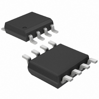
MAX4173TESA+ Maxim Integrated Products, MAX4173TESA+ Datasheet - Page 7

MAX4173TESA+
Manufacturer Part Number
MAX4173TESA+
Description
IC AMP CURR-SENSE HI-SIDE 8-SOIC
Manufacturer
Maxim Integrated Products
Datasheet
1.MAX4173EVKIT.pdf
(10 pages)
Specifications of MAX4173TESA+
Amplifier Type
Current Sense
Number Of Circuits
1
-3db Bandwidth
1.7MHz
Current - Input Bias
700µA
Voltage - Input Offset
300µV
Current - Supply
420µA
Voltage - Supply, Single/dual (±)
3 V ~ 28 V
Operating Temperature
-40°C ~ 85°C
Mounting Type
Surface Mount
Package / Case
8-SOIC (3.9mm Width)
Product
Current Monitors
Operating Temperature Range
+ 85 C
Mounting Style
SMD/SMT
Accuracy
2.5 %
Bandwidth
1.7 MHz
Sense Voltage (max)
150 mV
Supply Current (max)
0.42 mA (Typ) @ 28 V
Supply Voltage (max)
28 V
Supply Voltage (min)
3 V
No. Of Amplifiers
1
Input Bias Current
100µA
Input Offset Voltage
3mV
Cmrr
90dB
Supply Voltage Range
3V To 28V
Supply Current
420µA
Amplifier Case Style
SOIC
Rohs Compliant
Yes
Lead Free Status / RoHS Status
Lead free / RoHS Compliant
Output Type
-
Current - Output / Channel
-
Slew Rate
-
Gain Bandwidth Product
-
Lead Free Status / Rohs Status
Lead free / RoHS Compliant
The MAX4173 high-side current-sense amplifier fea-
tures a 0 to +28V input common-mode range that is
independent of supply voltage. This feature allows the
monitoring of current out of a battery in deep discharge
and also enables high-side current sensing at voltages
greater than the supply voltage (V
The MAX4173 operates as follows: Current from the
source flows through R
the internal-sense amplifier’s inverting input has high
impedance, negligible current flows through RG2
(neglecting the input bias current). Therefore, the
sense amplifier’s inverting-input voltage equals
V
gain forces its noninverting input to the same voltage as
the inverting input. Therefore, the drop across RG1
equals (I
I
multiplies I
I
RG1. Assuming infinite output impedance, V
(RGD). Substituting in for I
β
β
(I
MAX4173F, and GAIN = 100 for MAX4173H.
Figure 1. Functional Diagram
RG1
RGD
LOAD
SOURCE
·
·
(RGD / RG1)(R
RGD / RG1. Therefore, V
= (I
= β
+3V TO +28V
), where GAIN = 20 for MAX4173T, GAIN = 50 for
0 TO +28V
V
LOAD
SOURCE
LOAD
·
- (I
I
RG1
RG1
LOAD
)(R
)(R
V
CC
. Solving I
GND
SENSE
SENSE
by a current gain factor, β, to give
SENSE ·
)(R
CURRENT
MIRROR
I
RG1
SENSE
R
SENSE
RS+
) / RG1. The internal current mirror
Detailed Description
). Since I
G1
RGD = 12k
RGD
I
RGD
R
LOAD
SENSE
). The amplifier’s open-loop
MAX4173
A1
I
to the load (Figure 1). Since
RGD
OUT
and rearranging, V
= β
RG1
). The parts gain equals
OUT
Low-Cost, SOT23, Voltage-Output,
High-Side Current-Sense Amplifier
CC
R
I
RS-
LOAD
G2
= (GAIN) (R
·
).
flows through RG1,
(I
LOAD
TO LOAD BATTERY
V
OUT
OUT
)(R
SENSE
= (I
SENSE
OUT
RGD
) /
=
)
)
Set the full-scale output range by selecting R
the appropriate gain version of the MAX4173.
The MAX4173 senses a wide variety of currents with
different sense resistor values. Table 1 lists common
resistor values for typical operation of the MAX4173.
To measure lower currents more accurately, use a high
value for R
sense voltage that reduces offset voltage errors of the
internal op amp.
In applications monitoring very high currents, R
must be able to dissipate the I
rated power dissipation is exceeded, its value may drift
or it may fail altogether, causing a differential voltage
across the terminals in excess of the absolute maxi-
mum ratings.
If I
mize the inductance of R
have the highest inductance, metal-film resistors are
somewhat better, and low-inductance metal-film resis-
tors are best suited for these applications.
If the cost of R
critical, use the alternative solution shown in Figure 2.
This solution uses copper PC board traces to create a
sense resistor. The resistivity of a 0.1-inch-wide trace of
2-ounce copper is approximately 30mΩ/ft. The resis-
tance-temperature coefficient of copper is fairly high
(approximately 0.4%/°C), so systems that experience a
wide temperature variance must compensate for this
effect. In addition, do not exceed the maximum power
dissipation of the copper trace.
For example, the MAX4173T (with a maximum load cur-
rent of 10A and an R
V
R
wide copper trace.
The output of the MAX4173 is a current source driving a
12kΩ resistance. Resistive loading added to OUT
reduces the output gain of the MAX4173. To minimize
output errors for most applications, connect OUT to a
high-impedance input stage. When output buffering is
required, choose an op amp with a common-mode
input range and an output voltage swing that includes
ground when operating with a single supply. The op
SENSE
SENSE
SENSE
in this case requires about 2 inches of 0.1 inch-
of 50mV that yields a maximum V
has a large high-frequency component, mini-
Recommended Component Values
SENSE
SENSE
Applications Information
Using a PCB Trace as R
. The high value develops a higher
SENSE
is an issue and accuracy is not
SENSE
of 5mΩ) creates a full-scale
2
R losses. If the resistor’s
Output Impedance
. Wire-wound resistors
Choosing R
OUT
SENSE
SENSE
SENSE
SENSE
of 1V.
and


