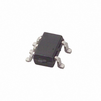
MAX4450EXK+T Maxim Integrated Products, MAX4450EXK+T Datasheet - Page 8

MAX4450EXK+T
Manufacturer Part Number
MAX4450EXK+T
Description
IC OP AMP R-R SGL 210MHZ SC70-5
Manufacturer
Maxim Integrated Products
Datasheet
1.MAX4450EUKT.pdf
(15 pages)
Specifications of MAX4450EXK+T
Amplifier Type
Voltage Feedback
Number Of Circuits
1
Output Type
Rail-to-Rail
Slew Rate
485 V/µs
-3db Bandwidth
210MHz
Current - Input Bias
6.5µA
Voltage - Input Offset
4000µV
Current - Supply
6.5mA
Current - Output / Channel
70mA
Voltage - Supply, Single/dual (±)
4.5 V ~ 11 V, ±2.25 V ~ 5.5 V
Operating Temperature
-40°C ~ 85°C
Mounting Type
Surface Mount
Package / Case
SC-70-5, SC-88A, SOT-323-5, SOT-353, 5-TSSOP
Number Of Channels
1
Voltage Gain Db
60 dB
Common Mode Rejection Ratio (min)
70 dB
Input Offset Voltage
4 mV
Operating Supply Voltage
5 V, 9 V
Maximum Power Dissipation
200 mW
Maximum Operating Temperature
+ 85 C
Mounting Style
SMD/SMT
Maximum Dual Supply Voltage
+/- 5.5 V
Minimum Operating Temperature
- 40 C
Lead Free Status / RoHS Status
Lead free / RoHS Compliant
Gain Bandwidth Product
-
Lead Free Status / Rohs Status
Details
Other names
MAX4450EXK+T
MAX4450EXK+TTR
MAX4450EXK+TTR
Ultra-Small, Low-Cost, 210MHz, Single-Supply
Op Amps with Rail-to-Rail Outputs
Table 1. Recommended Component Values
Note: R
0.1µF capacitor as close to the pin as possible. If operat-
ing with dual supplies, bypass each supply with a 0.1µF
capacitor.
Maxim recommends using microstrip and stripline tech-
niques to obtain full bandwidth. To ensure that the PC
board does not degrade the amplifier’s performance,
design it for a frequency greater than 1GHz. Pay care-
ful attention to inputs and outputs to avoid large para-
sitic capacitance. Whether or not you use a constant-
impedance board, observe the following design guide-
lines:
• Don’t use wire-wrap boards; they are too inductive.
• Don’t use IC sockets; they increase parasitic capaci-
• Use surface-mount instead of through-hole compo-
• Use a PC board with at least two layers; it should be
• Keep signal lines as short and as straight as possi-
The input common-mode range extends from
(V
mode rejection. Beyond this range, the amplifier output
is a nonlinear function of the input, but does not under-
go phase reversal or latchup.
The output swings to within 55mV of either power-
supply rail with a 2kΩ load. The input ground sensing
8
R
R
R
R
R
Small-Signal -3dB Bandwidth (MHz)
EE
F
G
S
TIN
TO
tance and inductance.
nents for better high-frequency performance.
as free from voids as possible.
ble. Do not make 90° turns; round all corners.
_______________________________________________________________________________________
(Ω)
(Ω)
(Ω)
(Ω)
- 200mV) to (V
(Ω)
following equation:
L
= R
COMPONENT
O
+ R
TO
CC
; R
TIN
- 2.25V) with excellent common-
R
TIN
and R
Ground-Sensing Input
Rail-to-Rail Outputs,
=
TO
1-
75
are calculated for 50Ω applications. For 75Ω systems, R
R
75
G
49.9
49.9
210
+1
24
—
Ω
∞
49.9
500
500
100
56
-1
0
49.9
49.9
500
500
+2
—
95
and the rail-to-rail output substantially increase the
dynamic range. With a symmetric input in a single +5V
application, the input can swing 2.95V
put can swing 4.9V
The MAX4450/MAX4451 are optimized for AC perfor-
mance. They are not designed to drive highly reactive
loads, which decrease phase margin and may produce
excessive ringing and oscillation. Figure 2 shows a cir-
cuit that eliminates this problem. Figure 3 is a graph of
the optimal isolation resistor (R
Figure 4 shows how a capacitive load causes exces-
sive peaking of the amplifier’s frequency response if
the capacitor is not isolated from the amplifier by a
resistor. A small isolation resistor (usually 20Ω to 30Ω)
placed before the reactive load prevents ringing and
oscillation. At higher capacitive loads, AC performance
is controlled by the interaction of the load capacitance
and the isolation resistor. Figure 5 shows the effect of a
27Ω isolation resistor on closed-loop response.
Coaxial cable and other transmission lines are easily
driven when properly terminated at both ends with their
characteristic impedance. Driving back-terminated
transmission lines essentially eliminates the line’s
capacitance.
49.9
500
250
62
50
-2
0
Output Capacitive Loading and Stability
49.9
49.9
500
124
+5
25
GAIN (V/V)
—
49.9
500
100
100
25
-5
0
P-P
with minimal distortion.
TO
49.9
49.9
+10
500
56
11
—
= 75Ω; calculate R
S
49.9
) vs. capacitive load.
500
-10
50
15
∞
0
P-P
49.9
49.9
+25
500
20
—
5
and the out-
TIN
from the
1200
49.9
-25
50
10
∞
0


