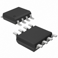
MAX4238ASA+ Maxim Integrated Products, MAX4238ASA+ Datasheet - Page 8

MAX4238ASA+
Manufacturer Part Number
MAX4238ASA+
Description
IC AMP LOW-NOISE 8-SOIC
Manufacturer
Maxim Integrated Products
Datasheet
1.MAX4238ATTT.pdf
(11 pages)
Specifications of MAX4238ASA+
Amplifier Type
General Purpose
Number Of Circuits
1
Output Type
Rail-to-Rail
Slew Rate
0.35 V/µs
Gain Bandwidth Product
1MHz
Current - Input Bias
1pA
Voltage - Input Offset
0.1µV
Current - Supply
600µA
Current - Output / Channel
40mA
Voltage - Supply, Single/dual (±)
2.7 V ~ 5.5 V
Operating Temperature
-40°C ~ 125°C
Mounting Type
Surface Mount
Package / Case
8-SOIC (3.9mm Width)
Lead Free Status / RoHS Status
Lead free / RoHS Compliant
-3db Bandwidth
-
Lead Free Status / Rohs Status
Lead free / RoHS Compliant
Autozeroing amplifiers typically require a substantial
amount of time to recover from an output overload. This
is due to the time it takes for the null amplifier to correct
the main amplifier to a valid output. The MAX4238/
MAX4239 require only 3.3ms to recover from an output
overload (see Electrical Characteristics and Typical
Operating Characteristics).
The MAX4238/MAX4239 feature a low-power (0.1µA)
shutdown mode. When SHDN is pulled low, the clock
stops and the device output enters a high-impedance
state. Connect SHDN to V
The MAX4238 is a unity-gain stable amplifier with a gain-
bandwidth product (GBWP) of 1MHz. The MAX4239 is
decompensated for a GBWP of 6.5MHz and is stable with
a gain of 10V/V. Unlike conventional operational ampli-
fiers, the MAX4238/MAX4239 have a maximum gain
specification. To maintain stability, set the gain of the
MAX4238 between A
gain of the MAX4239 between A
The low offset, fast settling time, and 1/f noise cancella-
tion of the MAX4238/MAX4239 make these devices
ideal for ADC buffers. The MAX4238/MAX4239 are well
suited for low-speed, high-accuracy applications such
as strain gauges (see Typical Application Circuit).
When using the MAX4238/MAX4239 as an ADC buffer,
the temperature drift should be taken into account when
determining the maximum input signal. With a typical off-
set drift of 10nV/°C, the drift over a 10°C range is 100nV.
Setting this equal to 1/2LSB in a 16-bit system yields a
full-scale range of 13mV. With a single 2.7V supply, an
acceptable closed-loop gain is A
sufficient gain while maintaining headroom.
Ultra-Low Offset/Drift, Low-Noise,
Precision SOT23 Amplifiers
8
_______________________________________________________________________________________
Applications Information
Minimum and Maximum Gain
Output Overload Recovery
V
= 1000V/V to 1V/V, and set the
CC
ADC Buffer Amplifier
for normal operation.
V
Error Budget Example
= 6700V/V and 10V/V.
V
= 200. This provides
Configurations
Shutdown
TRANSISTOR COUNT: 821
PROCESS: BiCMOS
SHDN
GND
IN+
IN-
1
2
4
3
TOP VIEW
*CONNECT EP TO GND.
MAX4238/
MAX4239
SO
+
(3mm x 3mm x 0.8mm)
8
7
6
5
EP*
6
1
N.C.
V
OUT
N.C.
CC
MAX4238/
MAX4239
Pin Configurations
TDFN
5
2
Chip Information
GND
OUT
IN+
4
3
1
2
3
MAX4238/
MAX4239
SOT23
6
5
4
V
SHDN
IN-
CC


