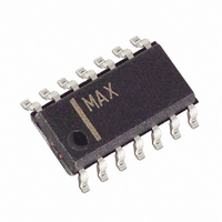
MAX4222ESD+ Maxim Integrated Products, MAX4222ESD+ Datasheet - Page 10

MAX4222ESD+
Manufacturer Part Number
MAX4222ESD+
Description
IC BUFFER CLOSED-LOOP R-R 14SOIC
Manufacturer
Maxim Integrated Products
Datasheet
1.MAX4222ESD.pdf
(16 pages)
Specifications of MAX4222ESD+
Amplifier Type
Buffer
Number Of Circuits
4
Output Type
Rail-to-Rail
Slew Rate
600 V/µs
-3db Bandwidth
200MHz
Current - Input Bias
5.4µA
Voltage - Input Offset
4000µV
Current - Supply
5.5mA
Current - Output / Channel
120mA
Voltage - Supply, Single/dual (±)
3.15 V ~ 11 V, ±1.575 V ~ 5.5 V
Operating Temperature
-40°C ~ 85°C
Mounting Type
Surface Mount
Package / Case
14-SOIC (3.9mm Width), 14-SOL
Number Of Channels
4
Voltage Gain Db
6.02 dB
Input Offset Voltage
4 mV (Typ) @ 5V
Operating Supply Voltage
5 V or 9 V
Supply Current
5.5 mA
Maximum Power Dissipation
667 mW
Mounting Style
SMD/SMT
Bandwidth
230 MHz
Input Bias Current (max)
5.4 uA (Typ) @ 5V
Maximum Operating Temperature
+ 85 C
Minimum Operating Temperature
- 40 C
Supply Voltage (max)
11 V
Supply Voltage (min)
3.15 V
Lead Free Status / RoHS Status
Lead free / RoHS Compliant
Gain Bandwidth Product
-
Lead Free Status / Rohs Status
Lead free / RoHS Compliant
As the load resistance decreases, the useful input range
is effectively limited by the output drive capability, since
the buffers have a fixed voltage gain of 2V/V or -1V/V.
For example, a 50
40mV above V
when operating from a single 5V supply. If the buffer is
operated in the noninverting, gain of 2V/V configuration
with the inverting input grounded, the useful input volt-
age range becomes 20mV to 1.7V instead of the
-100mV to 2.75V indicated by the Electrical Character-
istics. Beyond the useful input range, the buffer output
is a nonlinear function of the input, but it will not under-
go phase reversal or latchup.
The MAX4215/MAX4219 have an enable feature (EN_)
that allows the buffer to be placed in a low-power state.
When the buffers are disabled, the supply current is
reduced to 400µA per buffer.
As the voltage at the EN_ pin approaches the negative
supply rail, the EN_ input current rises. Figure 2 shows
a graph of EN_ input current versus EN_ pin voltage.
Figure 3 shows the addition of an optional resistor in
series with the EN pin, to limit the magnitude of the cur-
rent increase. Figure 4 displays the resulting EN pin
input current to voltage relationship.
The MAX4214/MAX4215/MAX4217/MAX4219/MAX4222
include internal protection circuitry that prevents dam-
age to the precision input stage from large differential
input voltages (Figure 5). This protection circuitry con-
High-Speed, Single-Supply, Gain of 2,
Closed-Loop, Rail-to-Rail Buffers with Enable
Figure 2. Enable Logic-Low Input Current vs. Enable Logic-
Low Threshold
10
______________________________________________________________________________________
-100
-120
-140
-160
-20
-40
-60
-80
20
0
EE
0
to 1.6V below V
Disabled Output Resistance
100
load can typically be driven from
V
IL
200
(mV ABOVE V
300
CC
EE
)
, or 40mV to 3.4V
400
500
Enable
sists of five back-to-back Schottky diodes between
IN_+ and IN_-. These diodes reduce the disabled out-
put resistance from 1k
age is 3V greater or less than the voltage at IN_+.
Under these conditions, the input protection diodes will
be forward biased, lowering the disabled output resis-
tance to 500 .
The MAX4214 family provides maximum AC perfor-
mance with no load capacitance. This is the case when
the load is a properly terminated transmission line.
These devices are designed to drive up to 20pF of load
capacitance without oscillating, but AC performance
will be reduced under these conditions.
Figure 3. Circuit to Reduce Enable Logic-Low Input Current
Figure 4. Enable Logic-Low Input Current vs. Enable Logic-
Low Threshold with 10k Series Resistor
Output Capacitive Loading and Stability
IN+
IN-
-10
-1
-2
-3
-4
-5
-6
-7
-8
-9
0
500
0
100
V
to 500
IL
MAX42_ _
200
(mV ABOVE V
ENABLE
500
EN_
10k
300
when the output volt-
EE
)
400
OUT
500


