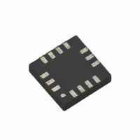
LMH6554LEE/NOPB National Semiconductor, LMH6554LEE/NOPB Datasheet - Page 13

LMH6554LEE/NOPB
Manufacturer Part Number
LMH6554LEE/NOPB
Description
IC OP AMP DIFF 2.8GHZ 14LLP
Manufacturer
National Semiconductor
Series
PowerWise®r
Datasheet
1.LMH6554LEENOPB.pdf
(16 pages)
Specifications of LMH6554LEE/NOPB
Amplifier Type
Differential
Number Of Circuits
1
Output Type
Differential
Slew Rate
6200 V/µs
-3db Bandwidth
2.8GHz
Current - Input Bias
1µA
Voltage - Input Offset
6500µV
Current - Supply
52mA
Current - Output / Channel
150mA
Voltage - Supply, Single/dual (±)
4.7 V ~ 5.25 V
Operating Temperature
-40°C ~ 125°C
Mounting Type
Surface Mount
Package / Case
14-LLP
No. Of Amplifiers
1
Input Offset Voltage
3mV
Bandwidth
2.8GHz
Supply Voltage Range
4.7V To 5.25V
Supply Current
52mA
Amplifier Case Style
LLP
No. Of Pins
14
Rohs Compliant
Yes
Lead Free Status / RoHS Status
Lead free / RoHS Compliant
Gain Bandwidth Product
-
Other names
LMH6554LEETR
Output Noise Performance and
Measurement
Unlike differential amplifiers based on voltage feedback ar-
chitectures, noise sources internal to the LMH6554 refer to
the inputs largely as current sources, hence the low input re-
ferred voltage noise and relatively higher input referred cur-
rent noise. The output noise is therefore more strongly
coupled to the value of the feedback resistor and not to the
closed loop gain, as would be the case with a voltage feed-
back differential amplifier. This allows operation of the
LMH6554 at much higher gain without incurring a substantial
noise performance penalty, simply by choosing a suitable
feedback resistor.
Figure 6
figure for the LMH6554 in a 50Ω system. A feedback resistor
value of 200Ω is chosen for the LLP package to minimize
output noise while simultaneously allowing both high gain (7
V/V) and proper 50Ω input termination. Refer to the section
titled Single Ended Input Operation for calculation of resistor
and gain values. Noise figure values at various frequencies
are shown in the plot titled Noise Figure in the Typical Per-
formance Characteristics section.
Driving Capacitive Loads
As noted previously, capacitive loads should be isolated from
the amplifier output with small valued resistors. This is par-
ticularly the case when the load has a resistive component
that is 500Ω or higher. A typical ADC has capacitive compo-
nents of around 10 pF and the resistive component could be
1000Ω or higher. If driving a transmission line, such as 50Ω
FIGURE 6. Noise Figure Circuit Configuration
FIGURE 5. Driving a 10-bit Gigasample ADC
shows a circuit configuration used to measure noise
30073261
30073266
13
coaxial or 100Ω twisted pair, using matching resistors will be
sufficient to isolate any subsequent capacitance. For other
applications see the Suggested R
charts in the Typical Performance Characteristics section.
Balanced Cable Driver
With up to 5.68 V
LMH6554 can be configured as a cable driver. The LMH6554
is also suitable for driving differential cables from a single
ended source as shown in
Power Supply Bypassing
The LMH6554 requires supply bypassing capacitors as
shown in
pacitors should be leadless SMT ceramic capacitors and
should be no more than 3 mm from the supply pins. These
capacitors should be star routed with a dedicated ground re-
turn plane or trace for best harmonic distortion performance.
Thin traces or small vias will reduce the effectiveness of by-
pass capacitors. Also shown in both figures is a capacitor from
the VCM and V
impedance and can provide a coupling path into the amplifier
for external noise sources, possibly resulting in loss of dy-
namic range, degraded CMRR, degraded balance and higher
distortion.
FIGURE 8. Split Supply Bypassing Capacitors
FIGURE 7. Fully Differential Cable Driver
Figure 8
EN
and
PP
pins to ground. These inputs are high
differential output voltage swing the
Figure
Figure
9. The 0.01 μF and 0.1 μF ca-
7.
OUT
vs. Capacitive Load
30073263
www.national.com
30073262


