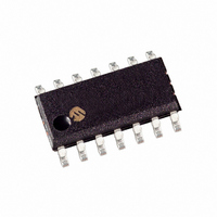
MCP604-E/SL Microchip Technology, MCP604-E/SL Datasheet - Page 14

MCP604-E/SL
Manufacturer Part Number
MCP604-E/SL
Description
IC OPAMP QUAD 2.7V 14SOIC
Manufacturer
Microchip Technology
Specifications of MCP604-E/SL
Slew Rate
2.3 V/µs
Amplifier Type
General Purpose
Number Of Circuits
4
Output Type
Rail-to-Rail
Gain Bandwidth Product
2.8MHz
Current - Input Bias
1pA
Voltage - Input Offset
700µV
Current - Supply
230µA
Current - Output / Channel
22mA
Voltage - Supply, Single/dual (±)
2.7 V ~ 6 V
Operating Temperature
-40°C ~ 125°C
Mounting Type
Surface Mount
Package / Case
14-SOIC (3.9mm Width), 14-SOL
Op Amp Type
Low Power
No. Of Amplifiers
4
Bandwidth
2.8MHz
Supply Voltage Range
2.7V To 6V
Amplifier Case Style
SOIC
No. Of Pins
14
Operating Temperature Range
-40°C To
Lead Free Status / RoHS Status
Lead free / RoHS Compliant
-3db Bandwidth
-
Lead Free Status / RoHS Status
Lead free / RoHS Compliant, Lead free / RoHS Compliant
Available stocks
Company
Part Number
Manufacturer
Quantity
Price
Company:
Part Number:
MCP604-E/SL
Manufacturer:
MICROCHIP
Quantity:
5 000
Part Number:
MCP604-E/SL
Manufacturer:
MICROCHIP/微芯
Quantity:
20 000
MCP6021/1R/2/3/4
After selecting R
resulting frequency response peaking and step
response overshoot. Modify R
response is reasonable. Evaluation on the bench and
simulations with the MCP6021/1R/2/3/4 Spice macro
model are helpful.
4.4
Figure 2-35 and Figure 2-36 use R
(frequency
response) overshoot. The capacitance to ground at the
inverting input (C
input capacitance plus board parasitic capacitance. C
is in parallel with R
at high frequencies for non-inverting gains greater than
1 V/V (unity gain). C
of the feedback loop for both non-inverting and
inverting gains.
FIGURE 4-4:
with parasitic capacitance.
The largest value of R
used is a function of noise gain (see G
“Capacitive Loads”) and C
for various conditions. Other compensation techniques
may be used, but they tend to be more complicated to
the design.
FIGURE 4-5:
with parasitic capacitance.
DS21685C-page 14
1.E+05
1.E+04
1.E+03
1.E+02
V
100k
10k
100
IN
1k
Gain Peaking
1
G
response)
C
N
C
G
G
> +1 V/V
= 20 pF
C
= 7 pF
ISO
G
G
G
) is the op amp’s common mode
, which causes an increase in gain
G
for your circuit, double-check the
Non-inverting gain circuit
Non-inverting gain circuit
also reduces the phase margin
Noise Gain; G
F
R
in Figure 4-4 that should be
gain
G
G
. Figure 4-5 shows results
R
F
ISO
peaking
N
’s value until the
(V/V)
F
= 1 k
N
C
C
in Section 4.3
G
G
= 50 pF
= 100 pF
V
and
OUT
to avoid
(step
10
G
4.5
The MCP6023 is a single amplifier with chip select
(CS). When CS is high, the supply current is less than
10 nA (typ) and travels from the CS pin to V
amplifier output being put into a high-impedance state.
When CS is low, the amplifier is enabled. If CS is left
floating, the amplifier may not operate properly.
Figure 1-1 and Figure 2-39 show the output voltage
and supply current response to a CS pulse.
4.6
The single op amps (MCP6021 and MCP6023), not in
the SOT-23-5 package, have an internal mid-supply
reference voltage connected to the V
Figure 4-6). The MCP6021 has CS internally tied to
V
provides a mid-supply reference. With the MCP6023,
taking the CS pin high conserves power by shutting
down both the op amp and the V
the CS pin low turns on the op amp and V
FIGURE 4-6:
circuit (MCP6021 and MCP6023 only).
See Figure 4-7 for a non-inverting gain circuit using the
internal
capacitor (C
amp input to the source.
FIGURE 4-7:
using V
SS
, which always keeps the op amp on and always
V
(CS tied internally to V
IN
REF
MCP6023 Chip Select (CS)
MCP6021 and MCP6023 Reference
Voltage
mid-supply
V
B
REF
(MCP6021 and MCP6023 only).
CS
) also reduces noise by coupling the op
R
C
G
B
Simplified internal V
Non-inverting gain circuit
reference.
© 2006 Microchip Technology Inc.
R
SS
V
F
REF
V
V
for MCP6021)
DD
SS
REF
The
50 k
50 k
circuitry. Taking
REF
REF
DC-blocking
V
SS
OUT
REF
, with the
pin (see
circuitry.


