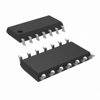
LM837M/NOPB National Semiconductor, LM837M/NOPB Datasheet - Page 2

LM837M/NOPB
Manufacturer Part Number
LM837M/NOPB
Description
IC OP AMP QUAD LOW NOISE 14-SOIC
Manufacturer
National Semiconductor
Specifications of LM837M/NOPB
Amplifier Type
General Purpose
Number Of Circuits
4
Slew Rate
10 V/µs
Gain Bandwidth Product
25MHz
Current - Input Bias
500nA
Voltage - Input Offset
300µV
Current - Supply
10mA
Current - Output / Channel
40mA
Voltage - Supply, Single/dual (±)
10 V ~ 36 V, ±5 V ~ 18 V
Operating Temperature
-40°C ~ 85°C
Mounting Type
Surface Mount
Package / Case
14-SOIC (3.9mm Width), 14-SOL
Bandwidth
25 MHz
Common Mode Rejection Ratio
100
Current, Input Bias
500 nA
Current, Input Offset
10 nA
Current, Output
40 mA
Current, Supply
10 mA
Harmonic Distortion
0.0015 %
Number Of Amplifiers
Quad
Package Type
MSOP-8
Power Dissipation
830 mW
Temperature, Operating, Range
-40 to +85 °C
Voltage, Gain
110 dB
Voltage, Input
10 to 36 V
Voltage, Noise
4.5 nV/sqrt Hz
Voltage, Offset
0.3 mV
Voltage, Output, High
13.5 V
Voltage, Output, Low
-13.5 V
Voltage, Supply
±15 V
Lead Free Status / RoHS Status
Lead free / RoHS Compliant
Output Type
-
-3db Bandwidth
-
Lead Free Status / Rohs Status
RoHS Compliant part
Electrostatic Device
Other names
*LM837M
*LM837M/NOPB
LM837M
*LM837M/NOPB
LM837M
www.national.com
V
I
I
A
V
V
CMRR
PSRR
I
SR
GBW
PBW
e
e
i
THD
f
φ
∆V
n
OS
B
S
U
Symbol
m
n1
n2
Absolute Maximum Ratings
If Military/Aerospace specified devices are required,
please contact the National Semiconductor Sales Office/
Distributors for availability and specifications.
DC Electrical Characteristics
T
OS
V
OM
CM
AC Electrical Characteristics
T
Design Electrical Characteristics
T
Symbol
Supply Voltage, V
Differential Input Voltage, V
2)
Common Mode Input Voltage, V
(Note 2)
Power Dissipation, P
Operating Temperature Range, T
Symbol
OS
A
A
A
= 25˚C, V
= 25˚C, V
= 25˚C, V
/∆T
Power Bandwidth
Equivalent Input Noise Voltage
Equivalent Input Noise Voltage
Equivalent Input Noise Current
Total Harmonic Distortion
Zero Cross Frequency
Phase Margin
Input-Referred Crosstalk
Average TC of Input Offset Voltage
S
Input Offset Voltage
Input Offset Current
Input Bias Current
Large Signal Voltage Gain
Output Voltage Swing
Common Mode Input Voltage
Common Mode Rejection Ratio
Power Supply Rejection Ratio
Power Supply Current
S
S
=
Slew Rate
Gain Bandwidth Product
±
=
=
15V (Note 4)
±
±
15V
15V
CC
/V
D
EE
(Note 3)
Parameter
Parameter
Parameter
ID
(Note
IC
OPR
−40˚C to +85˚C
830 mW (M)
R
f = 100 kHz, R
(Note 1)
L
1.2W (N)
= 600Ω
R
R
R
R
V
V
R
V
JIS A, R
f = 1 kHz
f = 1 kHz
A
f = 20 ∼ 20 kHz, R
Open Loop
Open Loop
f = 20 ∼ 20 kHz
S
L
L
L
IN
S
L
O
V
±
±
±
= 2 kΩ, V
= 2 kΩ
= 600Ω
=
= 15 ∼ 5, −15 ∼ −5
= 50Ω
= 1, V
18V
30V
15V
= 25 V
=
∞
±
Condition
, Four Amps
12V
S
Condition
OUT
P-P
= 100Ω
L
2
= 600Ω
OUT
, R
= 3 Vrms,
Condition
L
Storage Temperature Range, T
Soldering Information
ESD rating to be determined.
See AN-450 “Surface Mounting Methods and Their Effect
on Product Reliability” for other methods of soldering
surface mount devices.
=
= 600Ω, THD
L
Dual-In-Line Package
Small Outline Package
±
Soldering (10 seconds)
Vapor Phase (60 seconds)
Infrared (15 seconds)
= 600Ω
10V
Min
<
15
±
±
±
8
Min
90
80
80
1%
12
10
12
Min
Typ
±
±
±
10
25
Typ
500
110
100
100
0.3
13.5
12.5
14.0
10
10
STG
0.0015
−120
Typ
200
0.5
4.5
0.7
12
45
2
Max
1000
Max
−60˚C to +150˚C
200
15
5
Max
Units
260˚C
215˚C
220˚C
V/µs
MHz
Units
µV/˚C
Units
mV
mA
nA
nA
dB
dB
dB
MHz
kHz
deg
V
V
V
nV/
pA/
µV
dB
%


