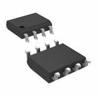
LM7121IM/NOPB National Semiconductor, LM7121IM/NOPB Datasheet - Page 14

LM7121IM/NOPB
Manufacturer Part Number
LM7121IM/NOPB
Description
IC AMP 175MHZ LP V FEEDBK 8-SOIC
Manufacturer
National Semiconductor
Datasheet
1.LM7121IM5NOPB.pdf
(19 pages)
Specifications of LM7121IM/NOPB
Amplifier Type
Voltage Feedback
Number Of Circuits
1
Slew Rate
1300 V/µs
Gain Bandwidth Product
175MHz
-3db Bandwidth
235MHz
Current - Input Bias
5.2µA
Voltage - Input Offset
900µV
Current - Supply
5.3mA
Current - Output / Channel
71mA
Voltage - Supply, Single/dual (±)
4.5 V ~ 33 V, ±2.25 V ~ 16.5 V
Operating Temperature
-40°C ~ 85°C
Mounting Type
Surface Mount
Package / Case
8-SOIC (3.9mm Width)
Number Of Channels
1
Voltage Gain Db
64 dB
Common Mode Rejection Ratio (min)
65 dB (Typ)
Input Offset Voltage
2.4 mV at 5 V (Typ)
Operating Supply Voltage
5 V, 9 V, 12 V, 15 V, 18 V, 24 V, 28 V
Supply Current
4.8 mA at 5 V (Typ)
Maximum Operating Temperature
+ 85 C
Maximum Dual Supply Voltage
+/- 16.5 V
Minimum Operating Temperature
- 40 C
Lead Free Status / RoHS Status
Lead free / RoHS Compliant
Output Type
-
Lead Free Status / Rohs Status
Details
Other names
*LM7121IM
*LM7121IM/NOPB
LM7121IM
*LM7121IM/NOPB
LM7121IM
www.national.com
Typical Performance Characteristics
Undistorted Output Swing
vs Frequency
Application Information
The table below, depicts the maximum operating supply volt-
age for each package type:
Stable unity gain operation is possible with supply voltage of
5V for all capacitive loads. This allows the possibility of using
the device in portable applications with low supply voltages
with minimum components around it.
Above a supply voltage of 6V (
tional resistor and capacitor (shown below) should be placed
in the feedback path to achieve stability at unity gain over the
full temperature range.
The package power dissipation should be taken into account
when operating at high ambient temperatures and/or high
power dissipative conditions. Refer to the power derating
curves in the data sheet for each type of package.
Single Supply
Dual Supplies
TABLE 1. Maximum Supply Voltage Values
FIGURE 1. Typical Circuit for A
Operation (V
SOT23-5
10V
±
5V
±
3V Dual supplies), an addi-
S
DS012348-87
6V)
SO-8
±
DS012348-86
30V
15V
V
= +1
T
Total Power Dissipation
vs Ambient Temperature
14
A
= 25˚C, R
In determining maximum operable temperature of the de-
vice, make sure the total power dissipation of the device is
considered; this includes the power dissipated in the device
with a load connected to the output as well as the nominal
dissipation of the op amp.
The device is capable of tolerating momentary short circits
from its output to ground but prolonged operation in this
mode will damage the device, if the maximum allowed junc-
tion temperation is exceeded.
APPLICATION CIRCUITS
Current Boost Circuit
The circuit in Figure 2 can be used to achieve good linearity
along with high output current capability.
By proper choice of R
supply a minimal amount of current, thereby improving its
output linearity.
R
R
The circuit above has been set for a load of 100 .
Reasonable speeds (
pected up to 120 mA
response across the load).
3
3
can be adjusted to allow for different loads:
= 0.1 R
FIGURE 2. Simple Circuit to Improve Linearity
L
= 1 M . unless otherwise specified (Continued)
L
and Output Drive Current
PP
<
3
30 ns rise and fall times) can be ex-
of load current (see Figure 3 for step
, the LM7121 output can be set to
DS012348-65
DS012348-92


