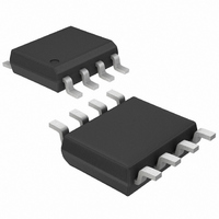
MAX4241ESA+ Maxim Integrated Products, MAX4241ESA+ Datasheet - Page 13

MAX4241ESA+
Manufacturer Part Number
MAX4241ESA+
Description
IC OP AMP BTR 8-SOIC
Manufacturer
Maxim Integrated Products
Series
Beyond-the-Rails™r
Datasheet
1.MAX4242ESA.pdf
(16 pages)
Specifications of MAX4241ESA+
Amplifier Type
General Purpose
Number Of Circuits
1
Output Type
Rail-to-Rail
Slew Rate
0.04 V/µs
Gain Bandwidth Product
90kHz
Current - Input Bias
2nA
Voltage - Input Offset
200µV
Current - Supply
14µA
Current - Output / Channel
2.5mA
Voltage - Supply, Single/dual (±)
1.8 V ~ 5.5 V, ±0.9 V ~ 2.5 V
Operating Temperature
-40°C ~ 85°C
Mounting Type
Surface Mount
Package / Case
8-SOIC (3.9mm Width)
Number Of Channels
1
Common Mode Rejection Ratio (min)
74 dB
Input Offset Voltage
0.75 mV
Input Bias Current (max)
6000 pA
Operating Supply Voltage
3 V, 5 V
Maximum Power Dissipation
471 mW
Maximum Operating Temperature
+ 85 C
Minimum Operating Temperature
- 40 C
Maximum Dual Supply Voltage
+/- 2.75 V
Minimum Dual Supply Voltage
+/- 0.9 V
Mounting Style
SMD/SMT
Shutdown
Yes
Supply Voltage (max)
5.5 V
Supply Voltage (min)
1.8 V
Voltage Gain Db
94 dB
Lead Free Status / RoHS Status
Lead free / RoHS Compliant
-3db Bandwidth
-
Lead Free Status / Rohs Status
Lead free / RoHS Compliant
value, based on driving the output voltage to within
50mV, 100mV, and 200mV of either power-supply rail.
For example, a MAX4241 running from a single +1.8V
supply, operating at T
within 100mV of V
load resistor to V
The same application can drive a 3.3kΩ load resistor
when terminated in V
The MAX4240–MAX4244 are unity-gain stable for loads
up to 200pF (see Load Resistor vs. Capacitive Load
graph in Typical Operating Characteristics ). Applica-
tions that require greater capacitive drive capability
should use an isolation resistor between the output and
the capacitive load (Figure 8). Note that this alternative
results in a loss of gain accuracy because R
voltage divider with the load resistor.
The MAX4240–MAX4244 family operates from either a
single +1.8V to +5.5V supply or dual ±0.9V to ±2.75V
supplies. For single-supply operation, bypass the
power supply with a 100nF capacitor to V
case GND). For dual-supply operation, both the V
Figure 8b. Pulse Response without Isolating Resistor
50mV/div
50mV/div
Power-Supply Bypassing and Layout
R
L
R
ISO
=
= NONE, R
1.8V - 0.1V
EE
______________________________________________________________________________________
CC
:
240 A
CC
L
A
and is capable of driving a 7k
= 100k , C
Driving Capacitive Loads
Single/Dual/Quad, +1.8V/10µA, SOT23,
= +25°C, can source 240µA to
/ 2 (+0.9V in this case).
100 s/div
L
= 700pF
7k to V
MAX4240-44 fig08b
EE
ISO
IN
OUT
EE
forms a
(in this
Beyond-the-Rails Op Amps
CC
and V
separate 100nF capacitors.
Good PC board layout techniques optimize perfor-
mance by decreasing the amount of stray capacitance
at the op amp’s inputs and output. To decrease stray
capacitance, minimize trace lengths by placing exter-
nal components as close as possible to the op amp.
Surface-mount components are an excellent choice.
Figure 8a Using a Resistor to Isolate a Capacitive Load from
the Op Amp
Figure 8c. Pulse Response with Isolating Resistor
EE
50mV/div
50mV/div
supplies should be bypassed to ground with
R
ISO
= 1k , R
MAX4240
MAX4241
MAX4242
MAX4243
MAX4244
L
= 100k , C
100 s/div
L
= 700pF
R
ISO
R
L
A
MAX4240-44 fig08c
V
=
R
L
R
+ R
L
ISO
C
IN
L
OUT
1
13


