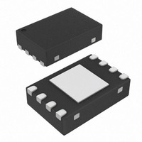
MCP6072T-E/MNY Microchip Technology, MCP6072T-E/MNY Datasheet - Page 17

MCP6072T-E/MNY
Manufacturer Part Number
MCP6072T-E/MNY
Description
IC OPAMP 1.2MHZ 1.8V 8-TDFN
Manufacturer
Microchip Technology
Specifications of MCP6072T-E/MNY
Amplifier Type
General Purpose
Number Of Circuits
2
Output Type
Rail-to-Rail
Slew Rate
0.5 V/µs
Gain Bandwidth Product
1.2MHz
Current - Input Bias
1pA
Voltage - Input Offset
150µV
Current - Supply
110µA
Current - Output / Channel
28mA
Voltage - Supply, Single/dual (±)
1.8 V ~ 6 V
Operating Temperature
-40°C ~ 125°C
Mounting Type
Surface Mount
Package / Case
8-TDFN
Lead Free Status / RoHS Status
Lead free / RoHS Compliant
-3db Bandwidth
-
Lead Free Status / Rohs Status
Lead free / RoHS Compliant
Other names
MCP6072T-E/MNYTR
Available stocks
Company
Part Number
Manufacturer
Quantity
Price
Company:
Part Number:
MCP6072T-E/MNY
Manufacturer:
MICRON
Quantity:
1 200
4.6
In applications where low input bias current is critical,
Printed Circuit Board (PCB) surface leakage effects
need to be considered. Surface leakage is caused by
humidity, dust or other contamination on the board.
Under low humidity conditions, a typical resistance
between nearby traces is 10
cause 5 pA of current to flow; which is greater than the
MCP6071/2/4 family’s bias current at +25°C (±1.0 pA,
typical).
The easiest way to reduce surface leakage is to use a
guard ring around sensitive pins (or traces). The guard
ring is biased at the same voltage as the sensitive pin.
An example of this type of layout is shown in
Figure
FIGURE 4-7:
for Inverting Gain.
1.
2.
© 2010 Microchip Technology Inc.
Non-inverting Gain and Unity-Gain Buffer:
a.Connect the non-inverting pin (V
b.Connect the guard ring to the inverting input
Inverting Gain and Transimpedance Gain
Amplifiers (convert current to voltage, such as
photo detectors):
a.Connect the guard ring to the non-inverting
b.Connect the inverting pin (V
Guard Ring
4-7.
PCB Surface Leakage
input with a wire that does not touch the
PCB surface.
pin (V
common mode input voltage.
input pin (V
to the same reference voltage as the op
amp (e.g., V
with a wire that does not touch the PCB
surface.
IN
–). This biases the guard ring to the
IN
DD
+). This biases the guard ring
Example Guard Ring Layout
/2 or ground).
V
IN
12
– V
Ω. A 5V difference would
IN
+
IN
–) to the input
V
IN
SS
+) to the
MCP6071/2/4
DS22142B-page 17


