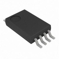
MCP6023T-I/ST Microchip Technology, MCP6023T-I/ST Datasheet - Page 3

MCP6023T-I/ST
Manufacturer Part Number
MCP6023T-I/ST
Description
IC OPAMP 2.5V R-R I/O 8TSSOP
Manufacturer
Microchip Technology
Datasheet
1.MCP6021-ESN.pdf
(42 pages)
Specifications of MCP6023T-I/ST
Amplifier Type
General Purpose
Number Of Circuits
1
Output Type
Rail-to-Rail
Slew Rate
7 V/µs
Gain Bandwidth Product
10MHz
Current - Input Bias
1pA
Voltage - Input Offset
500µV
Current - Supply
1mA
Current - Output / Channel
30mA
Voltage - Supply, Single/dual (±)
2.5 V ~ 5.5 V
Operating Temperature
-40°C ~ 85°C
Mounting Type
Surface Mount
Package / Case
8-TSSOP
Rohs Compliant
Yes
Lead Free Status / RoHS Status
Lead free / RoHS Compliant
-3db Bandwidth
-
Other names
MCP6023TI/ST
1.0
Absolute Maximum Ratings †
V
Current at Analog Input Pins (V
Analog Inputs (V
All Other Inputs and Outputs ......... V
Difference Input Voltage ...................................... |V
Output Short Circuit Current ................................ Continuous
Current at Output and Supply Pins ............................±30 mA
Storage Temperature ................................. –65° C to +150° C
Maximum Junction Temperature (T
ESD Protection On All Pins (HBM; MM) .............. ≥ 2 kV; 200V
DC ELECTRICAL CHARACTERISTICS
© 2009 Microchip Technology Inc.
Electrical Specifications: Unless otherwise indicated, T
V
Input Offset
Input Offset Voltage:
Input Offset Voltage Temperature Drift
Power Supply Rejection Ratio
Input Current and Impedance
Input Bias Current
Input Offset Current
Common-Mode Input Impedance
Differential Input Impedance
Common-Mode
Common-Mode Input Range
Common-Mode Rejection Ratio
Voltage Reference (MCP6021 and MCP6023 only)
V
V
Open-Loop Gain
DC Open-Loop Gain (Large Signal)
Output
Maximum Output Voltage Swing
Output Short Circuit Current
DD
OUT
REF
REF
Industrial Temperature Parts
Extended Temperature Parts
Extended Temperature Parts
Industrial Temperature Parts
Extended Temperature Parts
– V
Accuracy (V
Temperature Drift
≈ V
SS
ELECTRICAL
CHARACTERISTICS
DD
........................................................................7.0V
/2 and R
Parameters
IN
+, V
REF
L
IN
– V
= 10 kΩ to V
–) †† ........ V
DD
/2)
IN
+, V
J
)........................ .+150° C
DD
SS
SS
IN
/2.
–).....................±2 mA
– 1.0V to V
– 0.3V to V
ΔV
V
ΔV
V
CMRR
CMRR
CMRR
REF_ACC
OL
PSRR
Z
V
Sym
V
V
V
OS
Z
REF
A
I
I
I
DIFF
CMR
OS
I
I
I
SC
SC
CM
, V
OS
OS
OS
A
B
B
B
OL
/ΔT
/ΔT
OH
A
DD
DD
DD
+ 1.0V
+ 0.3V
– V
V
V
SS
SS
-500
-250
Min
-2.5
A
-50
SS
74
74
70
74
90
—
—
—
—
—
—
—
—
—
—
-0.3
+15
= +25°C, V
|
10
10
±100
±3.5
Typ
640
110
±30
±22
90
30
90
85
90
—
—
—
±1
—
—
—
13
13
1
DD
† Notice: Stresses above those listed under “Absolute
Maximum Ratings” may cause permanent damage to the
device. This is a stress rating only and functional operation of
the device at those or any other conditions above those
indicated in the operational listings of this specification is not
implied. Exposure to maximum rating conditions for extended
periods may affect device reliability.
†† See Section 4.1.2 “ Input Voltage and Current Limits”.
||6
||3
= +2.5V to +5.5V, V
V
V
5,000
DD
+500
+250
Max
+2.5
DD
150
+50
MCP6021/1R/2/3/4
—
—
—
—
—
—
—
—
—
—
—
—
—
+0.3
-20
µV/°C T
µV/°C T
Units
Ω||pF
Ω||pF
mV
mV
mV
mA
mA
µV
µV
dB
pA
pA
pA
pA
dB
dB
dB
dB
V
SS
V
V
V
T
V
T
T
V
V
V
V
V
0.5V input overdrive
V
V
= GND, V
A
A
A
A
A
CM
CM
CM
CM
DD
DD
DD
CM
OUT
DD
DD
= -40°C to +125°C
= -40°C to +125°C
= +85°C
= +125°C
= -40°C to +125°C
= 5V, V
= 5V, V
= 5V, V
= 2.5V
= 5.5V
= 0V
= 0V, V
= 0V, V
= 0V
= 0V,
= V
SS
CM
+0.3V to V
Conditions
CM
CM
CM
DD
DD
= V
= 5.0V
= 5.0V
= -0.3V to 5.3V
= 3.0V to 5.3V
= -0.3V to 3.0V
DD
DS21685D-page 3
/2,
DD
-0.3V


