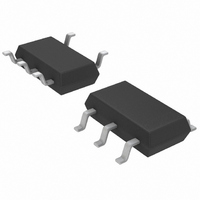
LT6220CS5#TRM Linear Technology, LT6220CS5#TRM Datasheet - Page 14

LT6220CS5#TRM
Manufacturer Part Number
LT6220CS5#TRM
Description
IC OPAMP PREC LP R-R TSOT23-5
Manufacturer
Linear Technology
Datasheet
1.LT6220CS5TRMPBF.pdf
(20 pages)
Specifications of LT6220CS5#TRM
Amplifier Type
General Purpose
Number Of Circuits
1
Output Type
Rail-to-Rail
Slew Rate
20 V/µs
Gain Bandwidth Product
60MHz
Current - Input Bias
250nA
Voltage - Input Offset
700µV
Current - Supply
1mA
Current - Output / Channel
50mA
Voltage - Supply, Single/dual (±)
2.2 V ~ 12.6 V, ±1.1 V ~ 6.3 V
Operating Temperature
0°C ~ 70°C
Mounting Type
Surface Mount
Package / Case
TSOT-23-5, TSOT-5, TSOP-5
Lead Free Status / RoHS Status
Contains lead / RoHS non-compliant
-3db Bandwidth
-
Other names
LT6220CS5#TRMTR
Available stocks
Company
Part Number
Manufacturer
Quantity
Price
APPLICATIO S I FOR ATIO
LT6220/LT6221/LT6222
A pair of complementary common emitter stages Q14/Q15
that enable the output to swing from rail-to-rail construct
the output stage. The capacitors C2 and C3 form the local
feedback loops that lower the output impedance at high
frequency. These devices are fabricated by Linear
Technology’s proprietary high speed complementary bi-
polar process.
Power Dissipation
The LT6222, with four amplifiers, is housed in a small
16-lead SSOP package and typically has a thermal resis-
tance (θ
die’s junction temperature does not exceed 150°C. The
junction temperature, T
temperature, T
tance, θ
The power dissipation in the IC is the function of the supply
voltage, output voltage and the load resistance. For a given
supply voltage, the worst-case power dissipation P
occurs when the maximum supply current and the output
voltage is at half of either supply voltage for a given load
resistance. P
Example: For an LT6222 in a 16-lead SSOP package
operating on ±5V supplies and driving a 100Ω load, the
worst-case power dissipation is given by:
If all four amplifiers are loaded simultaneously, then the
total power dissipation is 322mW.
The maximum ambient temperature at which the part is
allowed to operate is:
14
T
T
P
P
J
D MAX
D MAX
A
(
(
= T
= T
= 150°C – (0.322W • 135°C/W) = 106.5°C
JA
JA
A
J
:
)
)
) of 135°C/W. It is necessary to ensure that the
+ (P
– (P
/
=
Amp
D(MAX)
(
A
V I
D
D(MAX)
, power dissipation, P
S
• θ
=
=
•
U
(
0 018 0 0625 80 5
JA
S MAX
10 1 8
is given by:
.
(
)
• 135°C/W)
• .
J
, is calculated from the ambient
U
)
+
)
+
mA
.
⎛
⎜
⎝
V
)
2
S
+
⎞
⎟
⎠
W
( )
2
2 5
=
D
/
.
, and thermal resis-
R
L
2
.
/
mW
100
U
D(MAX)
Input Offset Voltage
The offset voltage will change depending upon which input
stage is active. The PNP input stage is active from the
negative supply rail to 1.2V below the positive supply rail,
then the NPN input stage is activated for the remaining
input range up to the positive supply rail during which the
PNP stage remains inactive. The offset voltage is typically
less than 70µV in the range that the PNP input stage is
active.
Input Bias Current
The LT6220/LT6221/LT6222 employ a patent pending
technique to trim the input bias current to less than 150nA
for the input common mode voltage of 0.2V above the
negative supply rail to 1.2V below the positive rail. The low
input offset voltage and low input bias current of the
LT6220/LT6221/LT6222 provide precision performance
especially for high source impedance applications.
Output
The LT6220/LT6221/LT6222 can deliver a large output
current, so the short-circuit current limit is set around
50mA to prevent damage to the device. Attention must be
paid to keep the junction temperature of the IC below the
absolute maximum rating of 150°C (refer to the Power
Dissipation section) when the output is in continuous
short circuit. The output of the amplifier has reverse-
biased diodes connected to each supply. If the output is
forced beyond either supply, unlimited current will flow
through these diodes. If the current is transient and limited
to several hundred milliamperes, no damage will occur to
the device.
Overdrive Protection
When the input voltage exceeds the power supplies, two
pair of crossing diodes, D1 to D4, will prevent the output
from reversing polarity. If the input voltage exceeds either
power supply by 700mV, diode D1/D2 or D3/D4 will turn
on to keep the output at the proper polarity. For the phase
reversal protection to perform properly, the input current
must be limited to less than 5mA. If the amplifier is
622012fa


