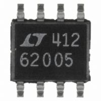
LT6200CS8-5#TR Linear Technology, LT6200CS8-5#TR Datasheet - Page 20

LT6200CS8-5#TR
Manufacturer Part Number
LT6200CS8-5#TR
Description
IC OP AMP 800MHZ R-R I/O 8-SOIC
Manufacturer
Linear Technology
Datasheet
1.LT6200CS6TRMPBF.pdf
(26 pages)
Specifications of LT6200CS8-5#TR
Amplifier Type
Buffer
Number Of Circuits
1
Output Type
Rail-to-Rail
Slew Rate
250 V/µs
Gain Bandwidth Product
800MHz
Current - Input Bias
23µA
Voltage - Input Offset
2500µV
Current - Supply
20mA
Current - Output / Channel
90mA
Voltage - Supply, Single/dual (±)
2.5 V ~ 12.6 V, ±1.25 V ~ 6.3 V
Operating Temperature
0°C ~ 70°C
Mounting Type
Surface Mount
Package / Case
8-SOIC (3.9mm Width)
Lead Free Status / RoHS Status
Contains lead / RoHS non-compliant
-3db Bandwidth
-
Available stocks
Company
Part Number
Manufacturer
Quantity
Price
APPLICATIONS INFORMATION
LT6200/LT6200-5
LT6200-10/LT6201
Amplifi er Characteristics
Figure 1 shows a simplifi ed schematic of the LT6200
family, which has two input differential amplifi ers in paral-
lel that are biased on simultaneously when the common
mode voltage is at least 1.5V from either rail. This topology
allows the input stage to swing from the positive supply
voltage to the negative supply voltage. As the common
mode voltage swings beyond V
saturates and current in Q1/Q4 is zero. Feedback is main-
tained through the Q2/Q3 differential amplifi er, but with
an input g
with I
1.5V of the negative rail. The effect of the g
a shift in the V
Input bias current normally fl ows out of the “+” and “–”
inputs. The magnitude of this current increases when the
input common mode voltage is within 1.5V of the negative
rail, and only Q1/Q4 are active. The polarity of this current
reverses when the input common mode voltage is within
1.5V of the positive rail and only Q2/Q3 are active.
The second stage is a folded cascode and current mir-
ror that converts the input stage differential signals to a
single ended output. Capacitor C1 reduces the unity cross
frequency and improves the frequency stability with-
out degrading the gain bandwidth of the amplifi er. The
differential drive generator supplies current to the output
transistors that swing from rail-to-rail.
20
2
when the common mode voltage swings within
m
reduction of one-half. A similar effect occurs
DESD1
DESD3
OS
–
+
D1
as I
–V
–V
1
or I
+V
+V
DESD2
D2
DESD4
2
saturate.
CC
– 1.5V, current source I
Q1
R3
R1
Q2
I
I
1
2
m
Q3
reduction is
Figure 1. Simplifi ed Schematic
R2
Q4
R4
1
Q8
Q5
C1
The LT6200-5/LT6200-10 are decompensated op amps
for higher gain applications. These amplifiers maintain
identical DC specifications with the LT6200, but have a
reduced Miller compensation capacitor C
in a significantly higher slew rate and gain bandwidth
product.
Input Protection
There are back-to-back diodes, D1 and D2, across the
+ and – inputs of these amplifiers to limit the differential
input voltage to ±0.7V. The inputs of the LT6200 family
do not have internal resistors in series with the input
transistors. This technique is often used to protect the
input devices from overvoltage that causes excessive
currents to flow. The addition of these resistors would
significantly degrade the low noise voltage of these
amplifiers. For instance, a 100Ω resistor in series with
each input would generate 1.8nV/√Hz of noise, and the
total amplifier noise voltage would rise from 0.95nV/√Hz
to 2.03nV/√Hz. Once the input differential voltage ex-
ceeds ±0.7V, steady-state current conducted though
the protection diodes should be limited to ±40mA.
This implies 25Ω of protection resistance per volt of
continuous overdrive beyond ±0.7V. The input diodes
are rugged enough to handle transient currents due to
amplifier slew rate overdrive or momentary clipping
without these resistors.
+V
Q9
R5
D3
Q7
Q6
BIAS
DIFFERENTIAL
C
GENERATOR
M
DRIVE
6203/04 F01
Q11
Q10
V –
–V
+V
DESD6
DESD7
DESD5
DESD8
–V
V
+
V
SHDN
M
. This results
62001fd


