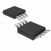
LT6001IMS8#TRPBF Linear Technology, LT6001IMS8#TRPBF Datasheet - Page 11

LT6001IMS8#TRPBF
Manufacturer Part Number
LT6001IMS8#TRPBF
Description
IC OP AMP DUAL R-R 8-MSOP
Manufacturer
Linear Technology
Datasheet
1.LT6000IDCBTRMPBF.pdf
(20 pages)
Specifications of LT6001IMS8#TRPBF
Amplifier Type
General Purpose
Number Of Circuits
2
Output Type
Rail-to-Rail
Slew Rate
0.018 V/µs
Gain Bandwidth Product
60kHz
Current - Input Bias
4nA
Voltage - Input Offset
400µV
Current - Supply
20µA
Current - Output / Channel
10mA
Voltage - Supply, Single/dual (±)
1.8 V ~ 16 V, ±0.9 V ~ 8 V
Operating Temperature
-40°C ~ 85°C
Mounting Type
Surface Mount
Package / Case
8-MSOP, Micro8™, 8-uMAX, 8-uSOP,
Lead Free Status / RoHS Status
Lead free / RoHS Compliant
-3db Bandwidth
-
Available stocks
Company
Part Number
Manufacturer
Quantity
Price
SI PLIFIED SCHE ATIC
APPLICATIO S I FOR ATIO
Supply Voltage
The positive supply of the LT6000/LT6001/LT6002 should
be bypassed with a small capacitor (about 0.01µF) within
an inch of the pin. When driving heavy loads, an additional
4.7µF electrolytic capacitor should be used. When using
split supplies, the same is true for the negative supply pin.
Rail-to-Rail Characteristics
The LT6000/LT6001/LT6002 are fully functional for an
input signal range from the negative supply to the positive
supply. Figure 1 shows a simplified schematic of the
amplifier. The input stage consists of two differential
amplifiers, a PNP stage Q3/Q6 and an NPN stage Q4/Q5
that are active over different ranges of the input common
mode voltage. The PNP stage is active for common mode
voltages, V
mately 1V below the positive supply. As V
towards the positive supply, the transistor Q7 will steer
Q2’s tail current to the current mirror Q8/Q9, activating the
NPN differential pair. The PNP pair becomes inactive for
V
Q16
–
SHDN
W
R8
7M
Q17
CM
Q18
, between the negative supply to approxi-
Q19
U
Q1
U
Q20
W
R1
Q8
Q7
IN
IN
+
–
W
V
V
+
+
CM
30k
30k
R2
R3
moves closer
D3
U
Figure 1
Q3
R6
Q4
the rest of the input common mode range up to the
positive supply.
The second stage is a folded cascode and current mirror
that converts the input stage differential signals into a
single ended output. Capacitor C1 reduces the unity cross
frequency and improves the frequency stability without
degrading the gain bandwidth of the amplifier. The comple-
mentary drive generator supplies current to the output
transistors that swing from rail to rail.
Input
The input bias current depends on which stage is active.
The input bias current polarity depends on the input
common mode voltage. When the PNP stage is active, the
input bias currents flow out of the input pins. They flow in
the opposite direction when the NPN stage is active. The
offset error due to the input bias currents can be
minimized by equalizing the noninverting and inverting
source impedance.
R4
Q9
Q2
Q5
R5
Q6
LT6000/LT6001/LT6002
R7
Q10
Q12
C1
Q11
Q13
DRIVE GENERATOR
COMPLEMENTARY
CM
Q14
Q15
11
V
–
600012fa
V
OUT
V
+
–


