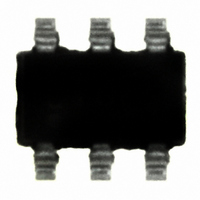
LT1809IS6#TRM Linear Technology, LT1809IS6#TRM Datasheet - Page 17

LT1809IS6#TRM
Manufacturer Part Number
LT1809IS6#TRM
Description
IC OPAMP R-R IN/OUT SNGL SOT23-6
Manufacturer
Linear Technology
Datasheet
1.LT1809CS6TRMPBF.pdf
(24 pages)
Specifications of LT1809IS6#TRM
Amplifier Type
General Purpose
Number Of Circuits
1
Output Type
Rail-to-Rail
Slew Rate
350 V/µs
Gain Bandwidth Product
180MHz
-3db Bandwidth
320MHz
Current - Input Bias
12.5µA
Voltage - Input Offset
800µV
Current - Supply
15mA
Current - Output / Channel
85mA
Voltage - Supply, Single/dual (±)
2.5 V ~ 12.6 V, ±1.25 V ~ 6.3 V
Operating Temperature
-40°C ~ 85°C
Mounting Type
Surface Mount
Package / Case
SOT-23-6
Lead Free Status / RoHS Status
Contains lead / RoHS non-compliant
Other names
LT1809IS6#TRMTR
Available stocks
Company
Part Number
Manufacturer
Quantity
Price
APPLICATIONS INFORMATION
Table 1. LT1809 6-Lead SOT-23 Package
Device is mounted on topside.
Table 2. LT1809/LT1810 SO-8 Package
Device is mounted on topside.
Table 3. LT1810 8-Lead MSOP Package
Device is mounted on topside.
Junction temperature T
temperature T
The power dissipation in the IC is the function of the
supply voltage, output voltage and the load resistance.
For a given supply voltage, the worst-case power dis-
sipation P
with the output voltage at half of either supply voltage (or
the maximum swing is less than 1/2 the supply voltage).
P
TOPSIDE
D(MAX)
TOPSIDE
(mm
(mm
T
P
1100
540
100
100
330
J
TOPSIDE (mm
30
D(MAX)
35
35
0
COPPER AREA
COPPER AREA
0
COPPER AREA
= T
2
2
)
)
A
is given by:
270
100
20
0
+ (P
D(MAX)
= (V
BACKSIDE
BACKSIDE
(mm
(mm
A
1100
D
540
100
330
2
35
0
0
0
S
0
0
and power dissipation P
)
• θ
2
2
• I
occurs at the maximum supply current
)
)
JA
S(MAX)
)
BOARD AREA
BOARD AREA
BOARD AREA
J
(mm
(mm
(mm
is calculated from the ambient
2500
2500
2500
2500
2500
2500
2500
2500
2500
2500
2500
2500
2500
2500
) + (V
2
2
2
)
)
)
S
/2)
(JUNCTION-TO-AMBIENT)
(JUNCTION-TO-AMBIENT)
(JUNCTION-TO-AMBIENT)
2
THERMAL RESISTANCE
THERMAL RESISTANCE
THERMAL RESISTANCE
/R
L
D
135°C/W
145°C/W
160°C/W
200°C/W
100°C/W
105°C/W
110°C/W
120°C/W
130°C/W
135°C/W
140°C/W
as follows:
65°C/W
85°C/W
95°C/W
Example: An LT1810 in SO-8 mounted on a 2500mm
of PC board without any extra heat spreading plane con-
nected to its V
θ
simultaneously driving 50Ω loads, the worst-case power
dissipation is given by:
The maximum ambient temperature that the part is al-
lowed to operate is:
To operate the device at higher ambient temperature, con-
nect more metal area to the V
resistance of the package as indicated in Table 2.
Input Offset Voltage
The offset voltage will change depending upon which
input stage is active and the maximum offset voltage is
guaranteed to be less than 3mV. The change of V
the entire input common mode range (CMRR) is less than
2.5mV on a single 5V and 3V supply.
Input Bias Current
The input bias current polarity depends upon a given input
common voltage at whichever input stage is operating.
When the PNP input stage is active, the input bias cur-
rents fl ow out of the input pins and fl ow into the input pins
when the NPN input stage is activated. Because the input
offset current is less than the input bias current, matching
the source resistances at the input pin will reduce total
offset error.
Output
The LT1809/LT1810 can deliver a large output current,
so the short-circuit current limit is set around 90mA to
prevent damage to the device. Attention must be paid to
keep the junction temperature of the IC below the absolute
maximum rating of 150°C (refer to the Power Dissipation
section) when the output is continuously short-circuited.
JA
P
T
. Operating on ± 5V supplies with both amplifi ers
A
D(MAX)
= T
= 150°C – (0.750W • 105°C/W) = 71°C
J
– (P
= 2 • (10 • 25mA) + 2 • (2.5)
= 0.5 + 0.250 = 0.750W
–
D(MAX)
pin has a thermal resistance of 105°C/W,
• 105°C/W)
LT1809/LT1810
–
pin to reduce the thermal
2
/50
OS
17
2
180910fa
over
area


