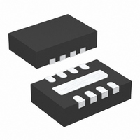
LT6014IDD#TR Linear Technology, LT6014IDD#TR Datasheet

LT6014IDD#TR
Specifications of LT6014IDD#TR
Available stocks
Related parts for LT6014IDD#TR
LT6014IDD#TR Summary of contents
Page 1
... LT6014 are both available in SO-8 and space saving 3mm × 3mm DFN packages. For unity gain stable ver- sions, refer to the LT6010 and LT6011 data sheets. , LTC and LT are registered trademarks of Linear Technology Corporation. All other trademarks are the property of their respective owners. LT6013/LT6014 0.1Hz to 10Hz Voltage Noise 5 • ...
Page 2
LT6013/LT6014 ABSOLUTE AXI U RATI GS + – Total Supply Voltage ( .............................. 40V Differential Input Voltage (Note 2) .......................... 10V Input Voltage .................................................... V Input Current (Note 2) ....................................... ±10mA Output Short-Circuit Duration ...
Page 3
ELECTRICAL CHARACTERISTICS temperature range, otherwise specifications are at T SYMBOL PARAMETER V Input Offset Voltage (Note 8) OS ∆V /∆T Input Offset Voltage Drift (Note Input Offset Current (Note Input Bias Current (Note 8) ...
Page 4
LT6013/LT6014 ELECTRICAL CHARACTERISTICS temperature range, otherwise specifications are at T SYMBOL PARAMETER i Input Noise Current Density n Input Noise Current (Low Frequency) Bandwidth = 0.01Hz to 1Hz R Input Resistance IN C Input Capacitance IN V Input Voltage Range ...
Page 5
ELECTRICAL CHARACTERISTICS temperature range, otherwise specifications are at T SYMBOL PARAMETER Offset Voltage Match (Note 7) ∆V OS Input Bias Current Match (Note 7) ∆I B Common Mode Rejection Ratio ∆CMRR Match (Note 7) Power Supply Rejection Ratio ∆PSRR Match ...
Page 6
LT6013/LT6014 ELECTRICAL CHARACTERISTICS temperature range, otherwise specifications are at T SYMBOL PARAMETER /∆T Input Offset Voltage Drift (Note 6) ∆ Input Offset Current (Note Input Bias Current (Note Input Noise Voltage Density ...
Page 7
ELECTRICAL CHARACTERISTICS temperature range, otherwise specifications are at T SYMBOL PARAMETER V Maximum Output Swing OUT + (Positive, Referred Maximum Output Swing – (Negative, Referred Output Short-Circuit Current SC (Note 3) SR Slew ...
Page 8
LT6013/LT6014 ELECTRICAL CHARACTERISTICS Note 1: Absolute Maximum Ratings are those beyond which the life of the device may be impaired. Note 2: The inputs are protected by back-to-back diodes and internal series resistors. If the differential input voltage exceeds 10V, ...
Page 9
W U TYPICAL PERFOR A CE CHARACTERISTICS Frequency n n CURRENT NOISE UNBALANCED SOURCE RESISTORS 1/f CORNER = 40Hz 10 1/f CORNER = 2Hz VOLTAGE NOISE 25° ...
Page 10
LT6013/LT6014 W U TYPICAL PERFOR A CE CHARACTERISTICS Supply Current vs Supply Voltage 500 PER AMPLIFIER 450 400 350 T = 85°C A 300 T = 25°C A 250 200 150 T = –40°C A 100 ...
Page 11
W U TYPICAL PERFOR A CE CHARACTERISTICS Output Impedance vs Frequency 1000 25°C A 100 100 0 0. ...
Page 12
LT6013/LT6014 U U APPLICATIO S I FOR ATIO Not Unity-Gain Stable The LT6013 and LT6014 amplifiers are optimized for the lowest possible noise and smallest package size, and are intentionally decompensated to be stable in a gain con- figuration of ...
Page 13
U U APPLICATIO S I FOR ATIO Preserving Input Precision Preserving the input accuracy of the LT6013 and LT6014 requires that the applications circuit and PC board layout do not introduce errors comparable to or greater than the 10µV typical ...
Page 14
LT6013/LT6014 PLIFIED SCHE ATIC + 500Ω – +IN R2 500Ω – (One Amplifier Q21 Q22 B A Q16 Q17 ...
Page 15
... MOLD FLASH OR PROTRUSIONS SHALL NOT EXCEED .006" (0.15mm) 2. DRAWING NOT TO SCALE Information furnished by Linear Technology Corporation is believed to be accurate and reliable. However, no responsibility is assumed for its use. Linear Technology Corporation makes no represen- tation that the interconnection of its circuits as described herein will not infringe on existing patent rights Package 8-Lead Plastic DFN (3mm × ...
Page 16
... Input Bias Current, Shutdown Feature www.linear.com ● 1/2 LT6014 2 – 49.9k 0.1µF 499Ω V OUT 499Ω 49.9k 6 – 7 – 1/2 LT6014 60134 TA02 V OUT I PHOTODIODE = 3.2µs r 60134 TA04 Up to 1000pF LT/LT 0305 REV B • PRINTED IN USA © LINEAR TECHNOLOGY CORPORATION 2004 60134fb ...


