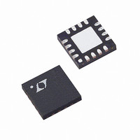
LT6402CUD-12#PBF Linear Technology, LT6402CUD-12#PBF Datasheet - Page 13

LT6402CUD-12#PBF
Manufacturer Part Number
LT6402CUD-12#PBF
Description
IC DIFF AMP/ADC DVR 12DB 16-QFN
Manufacturer
Linear Technology
Datasheet
1.LT6402IUD-12PBF.pdf
(16 pages)
Specifications of LT6402CUD-12#PBF
Amplifier Type
Differential
Number Of Circuits
2
Output Type
Differential
Slew Rate
400 V/µs
-3db Bandwidth
300MHz
Current - Input Bias
5µA
Voltage - Input Offset
1000µV
Current - Supply
30mA
Current - Output / Channel
35mA
Voltage - Supply, Single/dual (±)
4 V ~ 5.5 V, ±2 V ~ 2.5 V
Operating Temperature
0°C ~ 70°C
Mounting Type
Surface Mount
Package / Case
16-WQFN Exposed Pad
Lead Free Status / RoHS Status
Lead free / RoHS Compliant
Gain Bandwidth Product
-
Available stocks
Company
Part Number
Manufacturer
Quantity
Price
APPLICATIONS INFORMATION
can also be used, but since it is being driven differentially
it will appear at each fi ltered output as a single-ended
capacitance of twice the value. To halve the fi lter band-
width, for example, two 42pF capacitors could be added
(one from each fi ltered output to ground). Alternatively
one 21pF capacitor could be added between the fi ltered
outputs, again halving the fi lter bandwidth. Combinations
of capacitors could be used as well; a three capacitor
solution of 14pF from each fi ltered output to ground plus
a 14pF capacitor between the fi ltered outputs would also
halve the fi lter bandwidth (Figure 7).
Bandpass fi ltering is also easily implemented with just a
few external components. An additional 560pF and 62nH,
each added differentially between +OUTFILTERED and
–OUTFILTERED creates a bandpass fi lter with a 26MHz
center frequency, –3dB points of 23MHz and 30MHz, and
1.6dB of insertion loss (Figure 8).
Figure 8. LT6402-12 Output Filter Modifi ed for Bandpass
Filtering (1 External Inductor, 1 External Capacitor)
LT6402-12
LT6402-12
Figure 7. LT6402-12 Internal Filter Topology Modifi ed
for 1/2x Filter Bandwidth (3 External Capacitors)
50Ω
50Ω
50Ω
50Ω
14pF
14pF
14pF
14pF
14pF
14pF
V
V
V
V
EE
EE
EE
EE
8
7
6
5
8
7
6
5
640212 F08
640212 F07
–OUT
–OUTFILTERED
+OUTFILTERED
+OUT
–OUT
+OUT
–OUTFILTERED
+OUTFILTERED
14pF
14pF
14pF
FILTERED OUTPUT
FILTERED OUTPUT
(37.5MHz)
Output Common Mode Adjustment
The LT6402-12’s output common mode voltage is set by the
V
the output common mode voltage anywhere in a range
from 1.1V to 3.6V. Bandwidth of the V
200MHz, so for applications where the V
a DC bias voltage, a 0.1μF capacitor at this pin is recom-
mended. For best distortion performance, the voltage at
the V
When interfacing with most ADCs, there is generally a
V
of the ADC. For 5V ADCs such as the LTC17XX family, this
V
addition of a 0.1μF capacitor) to the input V
LT6402-12. For 3V ADCs such as the LTC22XX families,
the LT6402-12 will function properly using the 1.65V from
the ADC’s V
Dynamic Range (SFDR) and distortion performance can
be achieved by level-shifting the LTC22XX’s V
voltage up to at least 1.8V. This can be accomplished as
shown in Figure 9 by using a resistor divider between the
LTC22XX’s V
the LT6402-12’s V
common mode voltage above 1.9V, AC coupling capacitors
are recommended between the LT6402-12 and LTC22XX
ADCs because of the input voltage range constraints of
the ADC.
IF IN
OCM
OCM
OCM
0.1μF
150Ω
OCM
pin. It is a high-impedance input, capable of setting
output pin that is at about half of the supply voltage
output pin should be connected directly (with the
Figure 9. Level Shifting 3V ADC V
Improved SFDR
pin should be between 1.2V and 2.6V.
13
14
15
16
CM
CM
–INB
–INA
+INB
+INA
reference pin, but improved Spurious Free
output pin and V
+OUTFILTERED
–OUTFILTERED
LT6402-12
OCM
V
2
OCM
pin with a 0.1μF capacitor. For a
6
7
0.1μF
CC
10Ω
10Ω
CM
LT6402-12
and then bypassing
OCM
Voltage for
1
2
OCM
AIN
AIN
pin is typically
OCM
CM
+
–
pin is tied to
4.02k
11k
LTC22xx
reference
pin of the
31
V
3V
CM
13
1.5V
1.9V
640212fa
640212 F09


