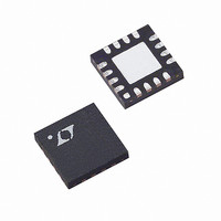
LT6402CUD-12#TRPBF Linear Technology, LT6402CUD-12#TRPBF Datasheet - Page 5

LT6402CUD-12#TRPBF
Manufacturer Part Number
LT6402CUD-12#TRPBF
Description
IC DIFF AMP/ADC DVR 12DB 16-QFN
Manufacturer
Linear Technology
Datasheet
1.LT6402IUD-12PBF.pdf
(16 pages)
Specifications of LT6402CUD-12#TRPBF
Amplifier Type
Differential
Number Of Circuits
2
Output Type
Differential
Slew Rate
400 V/µs
-3db Bandwidth
300MHz
Current - Input Bias
5µA
Voltage - Input Offset
1000µV
Current - Supply
30mA
Current - Output / Channel
35mA
Voltage - Supply, Single/dual (±)
4 V ~ 5.5 V, ±2 V ~ 2.5 V
Operating Temperature
0°C ~ 70°C
Mounting Type
Surface Mount
Package / Case
16-WQFN Exposed Pad
Lead Free Status / RoHS Status
Lead free / RoHS Compliant
Gain Bandwidth Product
-
Available stocks
Company
Part Number
Manufacturer
Quantity
Price
AC ELECTRICAL CHARACTERISTICS
⎯ E ⎯ N ⎯ A ⎯ B ⎯ L ⎯ E = 0.8V, +INA shorted to +INB (+IN), –INA shorted to –INB (–IN), V
unless otherwise noted.
SYMBOL
25MHz Signal
OIP3
NF
e
TYPICAL PERFORMANCE CHARACTERISTICS
Note 1: Stresses beyond those listed under Absolute Maximum Ratings
may cause permanent damage to the device. Exposure to any Absolute
Maximum Rating condition for extended periods may affect device
reliability and lifetime.
Note 2: As long as output current and junction temperature are kept below
the Absolute Maximum Ratings, no damage to the part will occur.
Note 3: The LT6402 is guaranteed functional over the operating
temperature range of –40°C to 85°C.
n25M
–12
–15
25M
18
15
12
–3
–6
–9
9
6
3
0
1
Frequency Response,
R
V
UNFILTERED: R
FILTERED: R
(EXTERNAL) + 100Ω
(INTERNAL, FILTERED OUTPUTS)
LOAD
IN
UNFILTERED OUTPUTS
= 50mV
FILTERED OUTPUTS
= 400Ω
PARAMETER
Second/Third Harmonic Distortion
Third-Order IMD
Output Third-Order Intercept
Noise Figure
Input Referred Noise Voltage Density
1dB Compression Point
P-P
LOAD
FREQUENCY (MHz)
10
LOAD
= 300Ω
= 400Ω
100
640212 G01
1000
24
21
18
15
12
–3
–6
6
0
9
3
CONDITIONS
2V
2V
2V
–OUTFILTERED), f1 = 24.5MHz, f2 = 25.5MHz
2V
R
Differential (+OUTFILTERED, –OUTFILTERED),
f1 = 24.5MHz, f2 = 25.5MHz (Note 5)
Measured Using DC954A Demo Board
R
1
Frequency Response vs C
R
L
L
V
UNFILTERED OUTPUTS
LOAD
P-P
P-P
P-P
P-P
IN
= 400Ω, f1 = 24.5MHz, f2 = 25.5MHz
= 100Ω (Note 5)
= 50V
Differential (+OUTFILTERED, –OUTFILTERED)
Differential (+OUT, –OUT)
Differential Composite (+OUTFILTERED,
Differential Composite (+OUT, –OUT),
0pF
1.6pF
5pF
10pF
= 400Ω
P-P
FREQUENCY (MHz)
10
T
A
= 25°C, V
Note 4: The LT6402C is guaranteed to meet specifi ed performance from
0°C to 70°C. It is designed, characterized and expected to meet specifi ed
performance from –40°C and 85°C but is not tested or QA sampled
at these temperatures. The LT6402I is guaranteed to meet specifi ed
performance from –40°C to 85°C.
Note 5: Since the LT6402-12 is a feedback amplifi er with low output
impedance, a resistive load is not required when driving an ADC.
Therefore, typical output power is very small. In order to compare the
LT6402-12 with typical g
LT6402-12 output voltage swing driving an ADC is converted to OIP3 and
P1dB as if it were driving a 50Ω load.
OCM
100
CCA
= 2.2V, Input common mode voltage = 2.2V, no R
LOAD
= V
640212 G02
,
CCB
1000
= V
CCC
m
amplifi ers that require 50Ω output loading, the
= 5V,V
–12
–15
–18
18
15
12
–3
–6
–9
6
3
0
9
1
Frequency Response,
R
V
UNFILTERED: R
FILTERED: R
(INTERNAL, FILTERED OUTPUTS)
LOAD
EEA
IN
MIN
UNFILTERED OUTPUTS
FILTERED OUTPUTS
= 50mV
= V
= 100Ω
EEB
P-P
LOAD
FREQUENCY (MHz)
10
15.1
13.5
TYP
–82
–73
–83
–74
= V
2.6
LOAD
40
LT6402-12
= 100Ω
EEC
= 100Ω
= 0V,
MAX
100
LOAD
640212 G03
nV/√Hz
640212fa
UNITS
5
dBm
dBm
1000
dBc
dBc
dBc
dBc
dB


