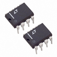
LT1413ACN8#PBF Linear Technology, LT1413ACN8#PBF Datasheet - Page 4

LT1413ACN8#PBF
Manufacturer Part Number
LT1413ACN8#PBF
Description
IC PRECISION OP-AMP DUAL 8-DIP
Manufacturer
Linear Technology
Datasheet
1.LT1413CN8PBF.pdf
(8 pages)
Specifications of LT1413ACN8#PBF
Amplifier Type
General Purpose
Number Of Circuits
2
Slew Rate
0.4 V/µs
Gain Bandwidth Product
950kHz
Current - Input Bias
8nA
Voltage - Input Offset
75µV
Current - Supply
350µA
Voltage - Supply, Single/dual (±)
2.85 V ~ 36 V, ±1.425 V ~ 18 V
Operating Temperature
0°C ~ 70°C
Mounting Type
Through Hole
Package / Case
8-DIP (0.300", 7.62mm)
Lead Free Status / RoHS Status
Lead free / RoHS Compliant
Output Type
-
Current - Output / Channel
-
-3db Bandwidth
-
Available stocks
Company
Part Number
Manufacturer
Quantity
Price
LT1413
V
V
The
temperature range.
Note 1: Typical parameters are defined as the 60% yield of parameter
distributions of individual amplifiers; i.e., out of 100 LT1413s typically 120
op amps will be better than the indicated specification.
Note 2: This parameter is tested on a sample basis only. All noise
parameters are tested with V
Note 3: This parameter is guaranteed by design and is not tested.
4
ELECTRICAL C
SYMBOL
V
I
I
CMRR
PSRR
A
V
SR
I
SYMBOL
V
I
I
A
CMRR
PSRR
I
SYMBOL
V
I
I
A
PSRR
I
CMRR
OS
B
S
OS
B
S
OS
B
S
OS
VOL
OS
VOL
OS
VOL
OUT
S
V
S
V
OS
OS
= 15V, 0 C T
= 15V, – 40 C T
/ T
/ T
denotes specifications which apply over the full operating
PARAMETER
Input Offset Voltage
Input Offset Voltage Drift
Input Offset Current
Input Bias Current
Large-Signal Voltage Gain
Common-Mode Rejection Ratio
Power Supply Rejection Ratio
Maximum Output Voltage Swing
Supply Current per Amplifier
PARAMETER
Input Offset Voltage
Input Offset Voltage Drift
Input Offset Current
Input Bias Current
Large-Signal Voltage Gain
Common-Mode Rejection Ratio
Power Supply Rejection Ratio
Maximum Output Voltage Swing
Supply Current per Amplifier
PARAMETER
Input Offset Voltage
Input Offset Current
Input Bias Current
Input Voltage Range
Common-Mode Rejection Ratio
Power Supply Rejection Ratio
Large-Signal Voltage Gain
Maximum Output Voltage Swing
Slew Rate
Supply Current per Amplifier
A
A
70 C, unless otherwise noted.
S
85 C (Note 7)
HARA TERISTICS
= 2.5V, V
O
C
= 0V.
CONDITIONS (Note 1)
LT1413N8
LT1413S8
(Note 5)
V
V
V
R
CONDITIONS (Note 1)
LT1413N8
LT1413S8
V
V
V
R
CONDITIONS (Note 1)
LT1413N8
LT1413S8
V
V
V
R
CM
S
O
O
CM
S
L
O
CM
S
L
L
= 2V to 18V
= 2V to 18V
= 10V, R
= 2k
= 10V, R
= 2k
= 10V, R
= 2k
= 13V, – 15V
= 13V, – 15V
2V to 18V
= 13.5V, – 15V
L
L
L
V
= 2k
= 2k
= 2k
S
= 15V, T
Note 4: Gain-Bandwidth Product is not tested. It is inferred from the slew
rate measurement.
Note 5: This parameter is not 100% tested.
Note 6: At the minimum supply voltage, the offset voltage changes less
than 200 V compared to its value at 5V, 0V.
Note 7: The LT1413 is not tested and is not quality-assurance sampled at
– 40 C and at 85 C. These specifications are guaranteed by design,
correlation and/or inference from 0 C, 25 C and/or 70 C tests.
A
= 25 C, unless otherwise noted.
– 15.0
1000
13.5
1500
MIN
MIN
MIN
100
103
101
800
100
0.2
12.5
12.2
98
97
13
LT1413ACN8
LT1413ACN8
LT1413ACN8
– 15.3
13.8
5000
4000
3000
TYP
TYP
116
119
360
TYP
100
115
118
370
117
120
350
0.4
0.1
0.4
0.2
0.1
0.4
13.9
13.8
75
95
10
9
8
14
MAX
MAX
MAX
280
500
390
550
460
580
2.5
1.0
2.8
1.4
0.7
20
25
15
– 15.0
13.5
1200
MIN
MIN
MIN
700
500
100
0.2
12.0
11.8
12.5
97
94
97
92
95
LT1413CN8/S8
LT1413CN8/S8
LT1413CN8/S8
– 15.3
4000
3000
2400
13.8
TYP
TYP
TYP
110
114
117
350
110
130
113
116
360
120
140
112
115
370
0.5
0.1
0.5
0.2
0.1
0.4
13.9
13.8
10
90
8
9
14
MAX
MAX
MAX
620
720
600
700
800
630
480
580
550
3.0
1.2
3.3
1.7
0.8
18
23
30
UNITS
UNITS
UNITS
V/mV
V/mV
V/mV
V/ C
V/ C
V/ s
nA
nA
dB
dB
nA
nA
dB
dB
nA
nA
dB
dB
V
V
V
A
V
V
V
A
V
V
V
V
V
A


