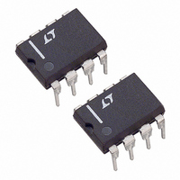
LT1001ACN8 Linear Technology, LT1001ACN8 Datasheet - Page 3

LT1001ACN8
Manufacturer Part Number
LT1001ACN8
Description
IC PRECISION OP-AMP SINGLE 8-DIP
Manufacturer
Linear Technology
Datasheet
1.LT1001CN8.pdf
(16 pages)
Specifications of LT1001ACN8
Amplifier Type
General Purpose
Number Of Circuits
1
Slew Rate
0.25 V/µs
Gain Bandwidth Product
800kHz
Current - Input Bias
500pA
Voltage - Input Offset
10µV
Voltage - Supply, Single/dual (±)
±3 V ~ 18 V
Operating Temperature
0°C ~ 125°C
Mounting Type
Through Hole
Package / Case
8-DIP (0.300", 7.62mm)
Lead Free Status / RoHS Status
Contains lead / RoHS non-compliant
Current - Supply
-
Output Type
-
Current - Output / Channel
-
-3db Bandwidth
-
Available stocks
Company
Part Number
Manufacturer
Quantity
Price
Company:
Part Number:
LT1001ACN8
Manufacturer:
LT
Quantity:
5 510
Company:
Part Number:
LT1001ACN8
Manufacturer:
NSC
Quantity:
5 510
Part Number:
LT1001ACN8
Manufacturer:
ST
Quantity:
20 000
Part Number:
LT1001ACN8#PBF
Manufacturer:
LINEAR/凌特
Quantity:
20 000
ELECTRICAL CHARACTERISTICS
temperature range, otherwise specifications are at T
SYMBOL PARAMETER
V
S
GBW
P
V
SYMBOL PARAMETER
V
I
I
A
CMRR
PSRR
V
P
Note 1: Absolute Maximum Ratings are those values beyond which the life
of a device may be impaired.
Note 2: Offset voltage for the LT1001AM/883 and LT1001AC are measured
after power is applied and the device is fully warmed up. All other grades
are measured with high speed test equipment, approximately 1 second
after power is applied. The LT1001AM/883 receives 168 hr. burn-in at
125 C. or equivalent.
Note 3: This parameter is tested on a sample basis only.
SYMBOL PARAMETER
V
I
I
A
CMRR
PSRR
V
P
V
OS
B
OS
B
OUT
R
d
OS
VOL
OUT
d
S
OS
VOL
OUT
d
S
Temp
Temp
V
V
= 15V, – 55 C T
= 15V, 0 C T
OS
OS
Input Voltage Range
Maximum Output Voltage Swing
Slew Rate
Gain-Bandwidth Product
Power Dissipation
Input Offset Voltage
Average Offset Voltage Drift
Input Offset Current
Input Bias Current
Large Signal Voltage Gain
Common Mode Rejection Ratio
Power Supply Rejection Ratio
Input Voltage Range
Output Voltage Swing
Power Dissipation
Input Offset Voltage
Average Offset Voltage Drift
Input Offset Current
Input Bias Current
Large Signal Voltage Gain
Common Mode Rejection Ratio
Power Supply Rejection Ratio
Input Voltage Range
Output Voltage Swing
Power Dissipation
A
A
70 C, unless otherwise noted
125 C, unless otherwise noted
CONDITIONS
R
R
R
(Note 5)
No load
No load, V
CONDITIONS
R
V
V
R
No load
CONDITIONS
R
V
V
R
No load
L
L
L
L
CM
S
L
CM
S
L
L
= 3V to 18V
= 3 to 18V
= 13V
= 13V
2k
1k
2k (Note 5)
2k , V
2k
2k , V
2k
S
A
= 3V
O
= 25 C. V
O
= 10V
= 10V
The
S
denotes the specifications which apply over the full operating
= 15V, T
Note 4: Long Term Input Offset Voltage Stability refers to the averaged
trend line of V
of operation. Excluding the initial hour of operation, changes in V
the first 30 days are typically 2.5 V.
Note 5: Parameter is guaranteed by design.
Note 6: 10Hz noise voltage density is sample tested on every lot. Devices
100% tested at 10Hz are available on request.
A
= 25 C, unless otherwise noted
MIN
MIN
MIN
12.5
13
13
12
300
110
104
13
350
110
106
13
12.5
0.1
0.4
LT1001AM/883
LT1001AM/883
OS
LT1001AC
LT1001AC
versus Time over extended periods after the first 30 days
TYP
0.25
0.8
46
4
TYP
14
14
13.5
TYP
0.7
14
13.8
0.2
0.5
750
124
120
50
0.2
0.8
1.0
20
14
13.5
30
700
122
117
55
MAX
MAX
MAX
0.6
3.5
3.5
0.6
4.0
60
85
60
4.0
90
75
6
MIN
MIN
MIN
200
106
100
250
106
103
13
13
12
13
12.0
13
12.5
0.1
0.4
LT1001M/LT1001C
LT1001M
LT1001C
TYP
TYP
TYP
0.3
0.6
48
4
700
120
117
14
1.0
14
14
13.5
0.3
1.2
13.5
30
45
60
750
123
120
0.25
0.8
14
13.8
55
1.5
MAX
MAX
MAX
110
160
100
1.0
5.3
8.0
5.5
1.0
7.6
90
80
8
LT1001
OS
during
UNITS
UNITS
UNITS
V/mV
1001fb
V/mV
3
V/ C
V/ s
MHz
V/ C
mW
mW
mW
mW
nA
nA
dB
dB
nA
nA
dB
dB
V
V
V
V
V
V
V
V
V


