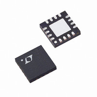
LTC6404HUD-4#PBF Linear Technology, LTC6404HUD-4#PBF Datasheet - Page 3

LTC6404HUD-4#PBF
Manufacturer Part Number
LTC6404HUD-4#PBF
Description
IC AMP/DRIVER DIFF 16-QFN
Manufacturer
Linear Technology
Type
ADC Driverr
Datasheet
1.LTC6404CUD-1PBF.pdf
(28 pages)
Specifications of LTC6404HUD-4#PBF
Applications
Data Acquisition
Mounting Type
Surface Mount
Package / Case
16-WQFN Exposed Pad
Current - Supply
31mA
Operating Temperature
-40°C ~ 125°C
Output Type
Differential, Rail-to-Rail
Number Of Circuits
1
Current - Output / Channel
85mA
Amplifier Type
Differential
Voltage - Supply, Single/dual (±)
2.7 V ~ 5.5 V, ±1.35 V ~ 2.75 V
-3db Bandwidth
530MHz
Slew Rate
1200 V/µs
Gain Bandwidth Product
1.7GHz
Current - Input Bias
23µA
Voltage - Input Offset
500µV
Lead Free Status / RoHS Status
Lead free / RoHS Compliant
Available stocks
Company
Part Number
Manufacturer
Quantity
Price
LTC6404 DC ELECTRICAL CHARACTERISTICS
the full operating temperature range, otherwise specifi cations are at T
V
R
V
SYMBOL
V
ΔV
I
ΔI
I
R
C
e
i
e
V
(Note 7)
CMRRI
(Note 8)
CMRRIO
(Note 8)
PSRR
(Note 9)
PSRRCM
(Note 9)
G
BAL
V
n
B
OS
n
nVOCM
SHDN
ICM
OSDIFF
IN
ICMR
OSCM
F
IN
CM
B
OSDIFF
= 200Ω. For the LTC6404-4: R
/ΔT
is defi ned (V
= OPEN, R
/ΔT Differential Offset Voltage Drift (Input Referred)
PARAMETER
Differential Offset Voltage (Input Referred)
Input Bias Current (Note 6)
Input Bias Current Drift (Note 6)
Input Offset Current (Note 6)
Input Resistance
Input Capacitance
Differential Input Referred Noise Voltage Density
Input Noise Current Density
Input Referred Common Mode Noise Voltage
Density
Input Signal Common Mode Range
Input Common Mode Rejection Ratio
(Input Referred) ΔV
Output Common Mode Rejection Ratio
(Input Referred) ΔV
Differential Power Supply Rejection
(ΔV
Output Common Mode Power Supply Rejection
(ΔV
Common Mode Gain (ΔV
Common Mode Gain Error
Output Balance (ΔV
Common Mode Offset Voltage (V
S
S
L
/ΔV
/ΔV
IN
= OPEN, R
+
OSDIFF
OSCM
+ V
IN
)
)
–
)/2. V
BAL
OUTCM
ICM
OCM
OUTDIFF
= 100k (See Figure 1). For the LTC6404-1: R
I
/ΔV
/ΔV
= 100Ω, R
OUTCM
/ΔV
OSDIFF
OSDIFF
OUTDIFF
is defi ned (V
/ΔV
OUTCM
OCM
F
)
= 402Ω, unless otherwise noted. V
)
– V
OCM
OUT
)
+
– V
CONDITIONS
V
V
V
V
V
Common Mode
Differential Mode
f = 1MHz
f = 1MHz
f = 1MHz, Referred to V
V
V
V
V
V
V
V
V
V
ΔV
ΔV
V
S
S
S
S
S
S
S
S
S
S
S
S
S
S
S
LTC6404-1
LTC6404-2
LTC6404-4
LTC6404-1
LTC6404-2
LTC6404-4
LTC6404-1
LTC6404-2
LTC6404-4
LTC6404-1
LTC6404-2
LTC6404-4
LTC6404-1
LTC6404-2
LTC6404-4
LTC6404-1
LTC6404-2
LTC6404-4
LTC6404-1
LTC6404-2
LTC6404-4
OUT
OUTDIFF
OUTDIFF
= 2.7V to 5.25V
= 2.7V to 5.25V
= 2.7V to 5.25V
= 2.7V to 5.25V
= 2.7V to 5.25V
= 3V
= 5V
= 3V, ΔV
= 5V, ΔV
= 5V, ΔV
= 2.7V to 5.25V
= 2.7V to 5.25V
= 5V, ΔV
= 5V, ΔV
= 2.7V to 5.25V
–
). V
= 2V, Single-Ended Input
= 2V, Differential Input
INDIFF
CM
CM
OCM
OCM
OCM
A
= 25°C. V
= 0.75V
= 1.25V
= 1V
= 1V
= 1V
= (V
I
= 100Ω, R
INP
OCM
S
+
The
is defi ned (V
– V
= 3V, V
Pin
INM
l
F
denotes the specifi cations which apply over
)
= 100Ω. For the LTC6404-2: R
–
= 0V, V
+
l
l
l
l
l
l
l
l
l
l
l
l
l
l
l
l
l
l
l
l
l
l
l
l
– V
CM
–
). V
= V
–0.6
–0.6
–1.6
MIN
–60
60
50
50
40
0
0
OCM
OUTCM
= V
–0.125
–0.25
1000
= (V
±0.5
0.01
10.5
0.99
TYP
–23
–60
–60
–53
–66
–66
–66
±10
±20
±40
1.5
±1
27
60
60
66
94
63
63
51
–1
ICM
1
3
1
3
9
1
1
LTC6404
OUT
= Mid-Supply,
+
I
+ V
MAX
±100
–0.4
= 100Ω,
±10
–40
–40
–40
–40
–40
–40
±25
±50
1.6
3.6
0.1
0.1
±2
0
OUT
–
)/2.
nV/√Hz
pA/√Hz
nV/√Hz
nV/√Hz
nV/√Hz
UNITS
μV/°C
μA/°C
3
6404f
V/V
V/V
V/V
mV
mV
mV
mV
kΩ
kΩ
μA
μA
dB
dB
dB
dB
dB
dB
dB
dB
dB
dB
dB
dB
dB
pF
%
%
%
V
V


