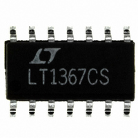
LT1367CS#TRPBF Linear Technology, LT1367CS#TRPBF Datasheet - Page 7

LT1367CS#TRPBF
Manufacturer Part Number
LT1367CS#TRPBF
Description
IC OP-AMP R-R IN/OUT QUAD 14SOIC
Manufacturer
Linear Technology
Datasheet
1.LT1368CN8PBF.pdf
(20 pages)
Specifications of LT1367CS#TRPBF
Amplifier Type
General Purpose
Number Of Circuits
4
Output Type
Rail-to-Rail
Slew Rate
0.13 V/µs
Gain Bandwidth Product
400kHz
Current - Input Bias
10nA
Voltage - Input Offset
200µV
Current - Supply
370µA
Current - Output / Channel
75mA
Voltage - Supply, Single/dual (±)
1.8 V ~ 30 V, ±0.9 V ~ 15 V
Operating Temperature
0°C ~ 70°C
Mounting Type
Surface Mount
Package / Case
14-SOIC (3.9mm Width), 14-SOL
Lead Free Status / RoHS Status
Lead free / RoHS Compliant
-3db Bandwidth
-
Available stocks
Company
Part Number
Manufacturer
Quantity
Price
elecTrical characTerisTics
SYMBOL
V
∆V
V
I
∆I
I
∆I
A
CMRR
PSRR
V
V
I
I
Note 1: Stresses beyond those listed under Absolute Maximum Ratings
may cause permanent damage to the device. Exposure to any Absolute
Maximum Rating condition for extended periods may affect device
reliability and lifetime.
Note 2: Applies to short circuits to ground for all split supplies and for
single supplies less than 20V. Short circuits to either supply for supplies
greater than 20V total may permanently damage the part. A heat sink may
be required to keep the junction temperature below the absolute maximum
rating when the output is shorted indefinitely.
temperature range of 0°C < T
B
OS
SC
S
VOL
OS
OS
OL
OH
B
OS
OS
TC
PARAMETER
Input Offset Voltage (LT1366/LT1368)
Input Offset Voltage (LT1367/LT1369)
Input Offset Voltage Shift (LT1366/LT1368)
Input Offset Voltage Match (Channel to Channel)
Input Offset Voltage Shift (LT1367/LT1369)
Input Offset Voltage Match (Channel to Channel)
Input Offset Voltage Drift
Input Bias Current
Input Bias Current Shift
Input Offset Current
Input Offset Current Shift
Input Bias Current Match (Channel to Channel)
Large-Signal Voltage Gain
Channel Separation
Common Mode Rejection Ratio (LT1366/LT1368)
CMRR Match (Channel to Channel)
Common Mode Rejection Ratio (LT1367/LT1369)
CMRR Match (Channel to Channel)
Power Supply Rejection Ratio
PSRR Match (Channel to Channel)
Output Voltage Swing Low
Output Voltage Swing High
Short-Circuit Current
Supply Current per Amplifier
A
< 70°C. V
S
= ±15V, V
CM
= 0V, V
CONDITIONS
V
V
V
V
V
V
V
V
(Note 3)
V
V
V
V
V
V
V
V
V
V
V
V
V
V
V
V
V
No Load
I
I
No Load
I
I
(Note 2)
SINK
SINK
SOURCE
SOURCE
CM
CM
CM
CM
CM
CM
CM
CM
CM
CM
CM
CM
CM
CM
CM
CM
O
O
O
CM
CM
CM
CM
S
S
= ±5V to ±15V
= ±5V to ±15V (Note 4)
= –14.7V to 14.7V, R
= –10V to 10V, R
= –10V to 10V, R
The
= V
= V
= V
= V
= V
= V
= V
= V
= V
= V
= V
= V
= V
= V
= V
= V
= V
= V
= V
= V
= 0.5mA
= 10mA
O
CC
EE
CC
EE
EE
EE
EE
EE
CC
EE
EE
CC
EE
EE
CC
EE
EE
EE
EE
EE
= 0.5mA
= 10mA
= 0V, unless otherwise noted.
l
, V
, V
to V
to V
to V
to V
(Note 4)
to V
to V
to V
to V
(Note 4)
denotes the specifications which apply over the specified
CC
CC
CC
CC
CC
CC
CC
CC
CC
CC
(Notes 4, 5)
(Notes 4, 5)
Note 3: This parameter is not 100% tested.
Note 4: Matching parameters are the difference between amplifiers A and
D and between B and C on the LT1367/LT1369; between the two amplifiers
on the LT1366/LT1368.
Note 5: Input offset voltage match is the difference in offset voltage
between amplifiers measured at both V
(Note 4)
(Note 4)
L
L
= 2k
= 2k
L
= 10k
l
l
l
l
l
l
l
l
l
l
l
l
l
l
l
l
l
l
l
l
l
l
l
l
l
l
l
l
l
l
l
l
l
l
V
V
V
CC
CC
CC
MIN
–45
750
500
110
±30
– 0.014
95
89
92
86
80
75
– 0.11
– 0.95
0
0
0
LT1366/LT1367
LT1368/LT1369
CM
V
V
V
V
V
V
CC
CC
CC
EE
EE
EE
= V
6000
6000
TYP
250
250
250
250
200
300
200
300
–10
135
103
103
103
103
105
100
415
+ 0.009
+ 0.045
+ 0.300
– 0.005
– 0.055
– 0.500
25
2
15
2
1
2
2
1
EE
and V
V
V
V
CM
EE
EE
EE
MAX
1150
1000
1500
2300
850
850
525
750
575
+ 0.014
+ 0.080
+ 0.600
= V
45
90
15
15
15
15
15
8
0
CC
.
UNITS
µV/°C
V/mV
V/mV
1366fb
mA
µV
µV
µV
µV
µV
µV
µV
µV
nA
nA
nA
nA
nA
nA
nA
nA
dB
dB
dB
dB
dB
dB
dB
µA
V
V
V
V
V
V


