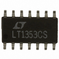
LT1353CS Linear Technology, LT1353CS Datasheet

LT1353CS
Specifications of LT1353CS
Available stocks
Related parts for LT1353CS
LT1353CS Summary of contents
Page 1
... Singles, duals and quads of each amplifier are available. The LT1352 is available in an 8-lead SO package. The LT1353 is offered in a 14-lead narrow surface mount package. , LTC and LT are registered trademarks of Linear Technology Corporation. C-Load is a trademark of Linear Technology Corporation. R4 50k – ...
Page 2
... A CM CONDITIONS f = 10kHz f = 10kHz V = 12V CM Differential V = 12V 2. 0. 2.5V to 15V S ORDER PART TOP VIEW NUMBER 14 OUT D 13 – LT1353CS 12 +IN D – + – OUT C S PACKAGE = 150 C, = 150 MIN TYP MAX SUPPLY 15V 0.2 0.6 5V 0.2 0.6 2.5V 0.3 ...
Page 3
ELECTRICAL CHARACTERISTICS SYMBOL PARAMETER A Large-Signal Voltage Gain VOL V Output Swing OUT I Output Current OUT I Short-Circuit Current SC SR Slew Rate Full-Power Bandwidth GBW Gain Bandwidth Rise Time, Fall Time r f Overshoot Propagation ...
Page 4
LT1352/LT1353 ELECTRICAL CHARACTERISTICS SYMBOL PARAMETER CMRR Common Mode Rejection Ratio PSRR Power Supply Rejection Ratio A Large-Signal Voltage Gain VOL V Output Swing OUT I Output Current OUT I Short-Circuit Current SC SR Slew Rate GBW Gain Bandwidth Channel Separation ...
Page 5
ELECTRICAL CHARACTERISTICS SYMBOL PARAMETER V Output Swing OUT I Output Current OUT I Short-Circuit Current SC SR Slew Rate GBW Gain Bandwidth Channel Separation I Supply Current S Note 1: Absolute Maximum Ratings are those values beyond which the life ...
Page 6
LT1352/LT1353 W U TYPICAL PERFORMANCE CHARACTERISTICS Input Bias Current vs Temperature 15V – 125 –50 ...
Page 7
W U TYPICAL PERFORMANCE CHARACTERISTICS Gain and Phase vs Frequency – PHASE 15V V = 15V ...
Page 8
LT1352/LT1353 W U TYPICAL PERFORMANCE CHARACTERISTICS Slew Rate vs Supply Voltage 200 – – ( )/2 150 100 50 0 ...
Page 9
W U TYPICAL PERFORMANCE CHARACTERISTICS Small-Signal Transient ( 1352/53 G31 Large-Signal Transient ( 1352/53 G34 U U APPLICATIONS INFORMATION Layout and Passive Components The LT1352/LT1353 amplifiers are easy to use and toler- ant of ...
Page 10
... C under certain conditions. Maximum junction temperature T ambient temperature T follows: LT1352CN8: T LT1352CS8: T LT1353CS: T Worst-case power dissipation occurs at the maximum supply current and when the output voltage is at 1/2 of either supply voltage (or the maximum swing if less than 1/2 supply voltage). For each amplifier P P ...
Page 11
PLIFIED SCHE ATIC + – – V Q11 Q10 + Q13 C T Q15 Q14 LT1352/LT1353 R2 R3 Q12 Q20 Q21 C1 R6 Q19 Q17 ...
Page 12
LT1352/LT1353 U TYPICAL APPLICATIONS DAC INPUTS DAC I-to-V Converter 10pF 12 5k – LT1352 565A TYPE + 5k V OUT ( < 0.5LSB OS A VOL 400kHz Photodiode Preamp with 10kHz Highpass Loop ...
Page 13
PACKAGE DESCRIPTION .300 – .325 (7.620 – 8.255) .008 – .015 (0.203 – 0.381) +.035 .325 –.015 +0.889 8.255 –0.381 NOTE: 1. DIMENSIONS ARE MILLIMETERS *THESE DIMENSIONS DO NOT INCLUDE MOLD FLASH OR PROTRUSIONS. MOLD FLASH OR PROTRUSIONS SHALL NOT ...
Page 14
LT1352/LT1353 PACKAGE DESCRIPTION .050 BSC .245 MIN .030 .005 TYP RECOMMENDED SOLDER PAD LAYOUT .010 – .020 (0.254 – 0.508) .008 – .010 (0.203 – 0.254) NOTE: 1. DIMENSIONS IN 2. DRAWING NOT TO SCALE 3. THESE DIMENSIONS DO NOT ...
Page 15
... MOLD FLASH OR PROTRUSIONS SHALL NOT EXCEED .006" (0.15mm) Information furnished by Linear Technology Corporation is believed to be accurate and reliable. However, no responsibility is assumed for its use. Linear Technology Corporation makes no represen- tation that the interconnection of its circuits as described herein will not infringe on existing patent rights. ...
Page 16
... LT1352 + 4700pF COMMENTS Good DC Precision, C-Load Stable, Power Saving Shutdown Good DC Precision, Stable with All Capacitive Loads www.linear.com 220pF – 1/2 V OUT LT1352 + 1352/53 TA04 LT/TP 0603 1K REV A • PRINTED IN USA LINEAR TECHNOLOGY CORPORATION 1996 13523fa ...


