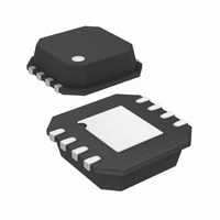
AD8137YCPZ-R2 Analog Devices Inc, AD8137YCPZ-R2 Datasheet

AD8137YCPZ-R2
Specifications of AD8137YCPZ-R2
Related parts for AD8137YCPZ-R2
AD8137YCPZ-R2 Summary of contents
Page 1
FEATURES Fully differential Extremely low power with power-down feature 2.6 mA quiescent supply current @ 5 V 450 µA in power-down mode @ 5 V High speed 110 MHz large signal 3 dB bandwidth @ 450 V/µs ...
Page 2
AD8137 TABLE OF CONTENTS Features .............................................................................................. 1 Applications ....................................................................................... 1 Functional Block Diagram .............................................................. 1 General Descripton .......................................................................... 1 Revision History ............................................................................... 2 Specifications ..................................................................................... 3 Absolute Maximum Ratings ............................................................ 6 Thermal Resistance ...................................................................... 6 Maximum Power Dissipation ..................................................... 6 ...
Page 3
SPECIFICATIONS V = ± 25°C, differential gain = OCM Table 1. Parameter DIFFERENTIAL INPUT PERFORMANCE Dynamic Performance −3 dB Small Signal Bandwidth −3 dB Large Signal Bandwidth Slew Rate Settling Time ...
Page 4
AD8137 2 25°C, differential gain = OCM Table 2. Parameter DIFFERENTIAL INPUT PERFORMANCE Dynamic Performance −3 dB Small Signal Bandwidth −3 dB Large Signal Bandwidth Slew Rate Settling Time ...
Page 5
1 25°C, differential gain = OCM Table 3. Parameter DIFFERENTIAL INPUT PERFORMANCE Dynamic Performance −3 dB Small Signal Bandwidth −3 dB Large Signal Bandwidth Slew Rate Settling Time to ...
Page 6
AD8137 ABSOLUTE MAXIMUM RATINGS Table 4. Parameter Supply Voltage V OCM Power Dissipation Input Common-Mode Voltage Storage Temperature Range Operating Temperature Range Lead Temperature (Soldering, 10 sec) Junction Temperature Stresses above those listed under Absolute Maximum Ratings may cause permanent ...
Page 7
PIN CONFIGURATION AND FUNCTION DESCRIPTIONS Table 6. Pin Function Descriptions Pin No. Mnemonic Description 1 −IN Inverting Input internal feedback loop drives the output common-mode voltage to be equal to the voltage applied to OCM the V ...
Page 8
AD8137 TYPICAL PERFORMANCE CHARACTERISTICS Unless otherwise noted, differential gain = 1, R Figure 60 for the definition of terms – –2 –3 –4 – –6 –7 –8 ...
Page 9
R = 1kΩ 2kΩ –1 –2 –3 –4 –5 –6 –7 –8 –9 –10 – 0.1V p – 100 FREQUENCY (MHz) ...
Page 10
AD8137 – 2kΩ –2 F –3 – 1kΩ F –5 –6 –7 – –9 = ± – 0.1V p – ...
Page 11
p –50 – 200Ω –70 – 500Ω – –100 –110 0.1 1 FREQUENCY (MHz) Figure 23. Second Harmonic Distortion at Various Loads – ...
Page 12
AD8137 – 500kHz p SECOND HARMONIC SOLID LINE –60 THIRD HARMONIC DASHED LINE –70 –80 –90 –100 –110 0.5 1.0 1.5 2.0 2.5 V (V) OCM Figure 29. Harmonic Distortion vs. V ...
Page 13
INPUT 6 OUTPUT –2 –4 –6 –8 TIME (ns) Figure 35. Overdrive Recovery 100 0pF 1pF –25 –50 – 100mV p-p ...
Page 14
AD8137 –5 PSRR = ∆V ∆V O, dm/ S –15 –25 –35 –PSRR –45 +PSRR –55 –65 –75 –85 0 FREQUENCY (MHz) Figure 41. PSRR vs. Frequency 1 0 –1 –2 –3 –4 –5 –6 – ...
Page 15
V OS OS, dm 0.1 0 –0.1 –0.2 –0.3 –40 – TEMPERATURE (°C) Figure 47. Offset Voltage vs. Temperature 1.2 1.0 0.8 0.6 0.4 0.2 0 –0.2 –0.4 0.50 1.50 2.50 ...
Page 16
AD8137 –1 = ± –2 –3 –4 –5 –5 –4 –3 –2 – OCM Figure 53. V vs. V Input Voltage O, cm OCM –20 –40 ...
Page 17
V = ± OCM –5 –4 –3 –2 – POWER-DOWN VOLTAGE (V) Figure 59. Supply Current vs. Power-Down Voltage Rev. D ...
Page 18
AD8137 TEST CIRCUITS V TEST TEST SIGNAL SOURCE V TEST TEST SIGNAL SOURCE R F 50Ω 1kΩ G 52.3Ω + AD8137 MIDSUPPLY V OCM 52.3Ω – 50Ω 1kΩ Figure ...
Page 19
THEORY OF OPERATION The AD8137 is a low power, low cost, fully differential voltage feedback amplifier that features a rail-to-rail output stage, common-mode circuitry with an internally derived common- mode reference voltage, and bias shutdown circuitry. The amplifier uses two ...
Page 20
AD8137 APPLICATIONS INFORMATION ANALYZING A TYPICAL APPLICATION WITH MATCHED R AND R NETWORKS F G Typical Connection and Definition of Terms Figure 64 shows a typical connection for the AD8137, using matched external R /R networks. The differential input F ...
Page 21
The differential output voltage noise contains contributions from the AD8137’s input voltage noise and input current noise as well as those from the external feedback networks. The contribution from the input voltage noise spectral density is computed as R ...
Page 22
AD8137 +2.5V V GND IN –2.5V The input impedance of a conventional inverting op amp configuration is simply R ; however higher in Equation 19 G because a fraction of the differential output voltage appears at the summing ...
Page 23
Estimating DC Errors Primary differential output offset errors in the AD8137 are due to three major components: the input offset voltage, the offset between the V and V input currents interacting with the AN AP feedback network resistances, and the ...
Page 24
AD8137 Figure 67 shows the AD8137 in a unity-gain configuration, and with the following discussion, provides a good example of how to provide a proper termination Ω environment. 0.1F 2V p-p 50 1k ...
Page 25
GND V 0 –10 –20 –30 –40 –50 –60 –70 –80 –90 –100 –110 –120 –130 –140 –150 –160 –170 100 FREQUENCY (kHz) Figure 70. AD8137 Performance on Single 5 V Supply, −1.82 dBFS ...
Page 26
AD8137 OUTLINE DIMENSIONS 0.25 (0.0098) 0.10 (0.0040) COPLANARITY PIN 1 INDICATOR 0.90 MAX 0.85 NOM SEATING PLANE 5.00 (0.1968) 4.80 (0.1890 6.20 (0.2441) 4.00 (0.1574) 1 5.80 (0.2284) 3.80 (0.1497) 4 1.27 (0.0500) BSC 1.75 (0.0688) 1.35 (0.0532) ...
Page 27
... AD8137YRZ −40°C to +125°C AD8137YRZ-REEL −40°C to +125°C AD8137YRZ-REEL7 −40°C to +125°C AD8137YCP-REEL –40°C to +125°C AD8137YCPZ-R2 –40°C to +125°C AD8137YCPZ-REEL –40°C to +125°C AD8137YCPZ-REEL7 –40°C to +125°C AD8137YCP-EBZ AD8137YR-EBZ RoHS Compliant Part ...
Page 28
AD8137 NOTES ©2004–2010 Analog Devices, Inc. All rights reserved. Trademarks and registered trademarks are the property of their respective owners. D04771-0-7/10(D) Rev Page ...


