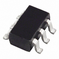
ADA4841-1YRJZ-R2 Analog Devices Inc, ADA4841-1YRJZ-R2 Datasheet - Page 15

ADA4841-1YRJZ-R2
Manufacturer Part Number
ADA4841-1YRJZ-R2
Description
IC OPAMP VF R-R LP LN SOT23-6
Manufacturer
Analog Devices Inc
Datasheet
1.ADA4841-1YRZ-R7.pdf
(20 pages)
Specifications of ADA4841-1YRJZ-R2
Slew Rate
13 V/µs
Amplifier Type
Voltage Feedback
Number Of Circuits
1
Output Type
Rail-to-Rail
-3db Bandwidth
80MHz
Current - Input Bias
3µA
Voltage - Input Offset
40µV
Current - Supply
1.5mA
Current - Output / Channel
60mA
Voltage - Supply, Single/dual (±)
2.7 V ~ 12 V, ±1.35 V ~ 6 V
Operating Temperature
-40°C ~ 125°C
Mounting Type
Surface Mount
Package / Case
SOT-23-6
Op Amp Type
Low Power
No. Of Amplifiers
1
Bandwidth
80MHz
Supply Voltage Range
2.7V To 12V
Amplifier Case Style
SOT-23
No. Of Pins
6
Lead Free Status / RoHS Status
Lead free / RoHS Compliant
Gain Bandwidth Product
-
Lead Free Status / RoHS Status
Lead free / RoHS Compliant, Lead free / RoHS Compliant
Figure 45 shows the amplifier frequency response as a G = −1
inverter with the input and output stage biased near the
negative supply rail.
The input voltage (V
0 V, (see Figure 39). +V
from −200 mV to −20 mV. With the input and output voltages
biased 200 mV above the bottom rail, the G = −1 inverter
frequency response is not much different from what is seen
with the input and output voltages biased near midsupply.
At 150 mV bias, the frequency response starts to decrease
and at 20 mV, the inverter bandwidth is less than half its
nominal value.
CAPACITANCE DRIVE
Capacitance at the output of an amplifier creates a delay within
the feedback path that, if within the bandwidth of the loop, can
create excessive ringing and oscillation. The G = +1 follower
topology has the highest loop bandwidth of any typical
configuration and, therefore, is the most vulnerable to the
effects of capacitance load.
A small resistor in series with the amplifier output and the
capacitive load mitigates the problem. Figure 46 plots the
recommended series resistance vs. capacitance for gains
of +1, +2, and +5.
Figure 45. Small Signal Frequency Response vs. Negative Supply Bias
–12
–3
–6
–9
6
3
0
0.1
V
G = –1
V
S+
IN
= 20mV p-p
= 5V
V
IN
S–
) and reference voltage (V
S
= –50mV
is biased at +5 V, and −V
1
FREQUENCY (MHz)
V
V
S–
S–
= –20mV
= –100mV
10
V
S–
= –150mV
V
IP
S–
) are both at
S
is swept
= –200mV
100
Rev. E | Page 15 of 20
INPUT PROTECTION
The ADA4841-1/ADA4841-2 are fully protected from ESD
events, withstanding human body model ESD events of 2.5 keV
and charge device model events of 1 keV with no measured
performance degradation. The precision input is protected
with an ESD network between the power supplies and diode
clamps across the input device pair, as shown in Figure 47.
For differential voltages above approximately 1.4 V, the diode
clamps start to conduct. Too much current can cause damage
due to excessive heating. If large differential voltages need to be
sustained across the input terminals, it is recommended that the
current through the input clamps be limited to below 150 mA.
Series input resistors sized appropriately for the expected
differential overvoltage provide the needed protection.
The ESD clamps start to conduct for input voltages more than
0.7 V above the positive supply and input voltages more than
0.7 V below the negative supply. It is recommended that the
fault current be limited to less than 150 mA if an overvoltage
condition is expected.
60
50
40
30
20
10
0
10
Figure 46. Series Resistance vs. Capacitance Load
VCC
VEE
Figure 47. Input Stage and Protection Diodes
VP
ESD
ESD
TO REST OF AMPLIFIER
G = +2
BIAS
CAPACITANCE LOAD (pF)
100
ADA4841-1/ADA4841-2
G = +1
G = +5
1000
ESD
ESD
VN
10000


