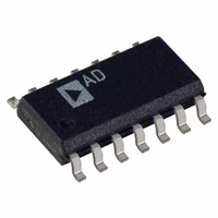
OP484FS Analog Devices Inc, OP484FS Datasheet - Page 19

OP484FS
Manufacturer Part Number
OP484FS
Description
IC OPAMP GP R-R 4.25MHZ 14SOIC
Manufacturer
Analog Devices Inc
Datasheet
1.OP184FSZ.pdf
(24 pages)
Specifications of OP484FS
Slew Rate
4 V/µs
Rohs Status
RoHS non-compliant
Amplifier Type
General Purpose
Number Of Circuits
4
Output Type
Rail-to-Rail
Gain Bandwidth Product
4.25MHz
Current - Input Bias
80nA
Voltage - Input Offset
250µV
Current - Supply
2.25mA
Current - Output / Channel
10mA
Voltage - Supply, Single/dual (±)
3 V ~ 36 V, ±1.5 V ~ 18 V
Operating Temperature
-40°C ~ 125°C
Mounting Type
Surface Mount
Package / Case
14-SOIC (3.9mm Width), 14-SOL
No. Of Amplifiers
4
Bandwidth
4.25MHz
No. Of Pins
14
Peak Reflow Compatible (260 C)
No
Input Bias Current
80nA
Input Offset Voltage Max
0.15mV
Leaded Process Compatible
No
-3db Bandwidth
-
Lead Free Status / RoHS Status
Contains lead / RoHS non-compliant
Available stocks
Company
Part Number
Manufacturer
Quantity
Price
Part Number:
OP484FS
Manufacturer:
ADI/亚德诺
Quantity:
20 000
Part Number:
OP484FSZ
Manufacturer:
ADI/亚德诺
Quantity:
20 000
Company:
Part Number:
OP484FSZ-REEL
Manufacturer:
ST
Quantity:
9 121
Part Number:
OP484FSZ-REEL7
Manufacturer:
ADI/亚德诺
Quantity:
20 000
LOW DROPOUT REGULATOR WITH CURRENT
LIMITING
Many circuits require stable, regulated voltages relatively close
in potential to an unregulated input source. This low dropout
type of regulator is readily implemented with a rail-to-rail output
op amp, such as the OP284, because the wide output swing allows
easy drive to a low saturation voltage pass device. Furthermore,
it is particularly useful when the op amp also employs a rail-to-
rail input feature because this factor allows it to perform high-
side current sensing for positive rail current limiting. Typical
examples are voltages developed from 3 V to 9 V range system
sources or anywhere that low dropout performance is required
for power efficiency. This 4.5 V example works from 5 V nominal
sources with worst-case levels down to 4.6 V or less. Figure 58
shows such a regulator set up, using an OP284 plus a low R
P-channel MOSFET pass device. Part of the low dropout perform-
ance of this circuit is provided by Q1, which has a rating of 0.11
Ω with a gate drive voltage of only 2.7 V. This relatively low gate
drive threshold allows operation of the regulator on supplies as
low as 3 V without compromising overall performance.
The main voltage control loop operation of the circuit is
provided by U1B, half of the OP284. This voltage control
amplifier amplifies the 2.5 V reference voltage produced by
Three Terminal U2, a REF192. The regulated output voltage,
V
OUT
, is then
V
OUT
=
CMOS HI (OR OPEN) = ON
ON/OFF CONTROL INPUT
V
V
OUT
IN
V
COMMON
S
2
OPTIONAL
> V
LO = OFF
⎛ +
⎜
⎝
1
OUT
+V
V
S
C
R2
R
+ 0.1V
3
⎞
⎟
⎠
0.1µF
C2
AD589
D2
R9
27.4kΩ
4.99kΩ
3
1N4148
301kΩ
D3
R7
R8
Figure 58. Low Dropout Regulator with Current Limiting
2
4
REF192
0.05Ω
6
R
R11
1kΩ
U2
S
1kΩ
R10
DS(ON)
R6
4.99kΩ
0.01µF
C5
3
2
Rev. I | Page 19 of 24
1µF
,
C2
8
4
OP284
R1
4.53kΩ
U1A
1
C4
0.1µF
V
2.5V
OUT2
For this example, because V
a U1B gain of 1.8 times, R3 and R2 are chosen for a ratio of 1.2:1 or
10.0 kΩ:8.06 kΩ (using closest 1% values). Note that for the lowest
V
this example), and the R2 to R3 resistors should be stable, close
tolerance metal film types. The table in Figure 58 summarizes
R1 to R3 values for some popular voltages. However, note that,
in general, the output can be anywhere between V
12 V maximum rating of Q1.
While the low voltage saturation characteristic of Q1 is a key part
of the low dropout, another component is a low current sense com-
parison threshold with good dc accuracy. Here, this is provided by
Current Sense Amplifier U1A, which is provided by a 20 mV
reference from the 1.235 V,
R7 to R8 divider. When the product of the output current and the
R
activated, and U1A drives the Q1 gate through D1. This causes the
overall circuit operation to enter current mode control with a
current limit, I
S
OUT
value match this voltage threshold, the current control loop is
1N4148
D1
I
R3
10kΩ
dc error, R2||R3 should be maintained equal to R1 (as in
6
5
LIMIT
0.01µF
C1
V
5.0V
4.5V
3.3V
3.0V
=
OUT
OP284
U1B
⎛
⎜
⎜
⎝
7
V
LIMIT
OUTPUT TABLE
R
R
R1kΩ
4.99
4.53
2.43
1.69
(
R5
22.1kΩ
R4
2.21kΩ
D2
S
, defined as
)
⎞
⎟
⎟
⎠
⎛
⎜
⎝
8.06kΩ
R2kΩ
10.0
8.08
3.24
2.00
SI9433DY
R
R2
7
Q1
R7
+
OUT
AD589
R8
R3kΩ
10.0
10.0
10.0
10.0
of 4.5 V with V
OP184/OP284/OP484
⎞
⎟
⎠
Reference Diode D2, and the
C6
10µF
V
4.5V @ 350mA
(SEE TABLE)
V
OUT
OUT
=
COMMON
OUT2
= 2.5 V requires
OUT2
and the


