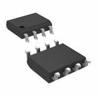
LME49870MAX/NOPB National Semiconductor, LME49870MAX/NOPB Datasheet - Page 4

LME49870MAX/NOPB
Manufacturer Part Number
LME49870MAX/NOPB
Description
IC AMP AUDIO MONO AB HIFI 8SOIC
Manufacturer
National Semiconductor
Datasheet
1.LME49870MABD.pdf
(34 pages)
Specifications of LME49870MAX/NOPB
Amplifier Type
Audio
Number Of Circuits
1
Slew Rate
20 V/µs
Gain Bandwidth Product
55MHz
Current - Input Bias
10nA
Voltage - Input Offset
140µV
Current - Supply
5mA
Current - Output / Channel
37mA
Voltage - Supply, Single/dual (±)
5 V ~ 44 V, ±2.5 V ~ 22 V
Operating Temperature
-40°C ~ 85°C
Mounting Type
Surface Mount
Package / Case
8-SOIC (3.9mm Width)
Number Of Channels
1
Voltage Gain Db
140 dB
Common Mode Rejection Ratio (min)
110 dB
Input Offset Voltage
0.7 mV at +/- 22 V
Maximum Operating Temperature
+ 85 C
Maximum Dual Supply Voltage
+/- 22 V
Minimum Operating Temperature
- 40 C
For Use With
LME49870MABD - BOARD EVAL 44V HP HIGH FIDEL
Lead Free Status / RoHS Status
Lead free / RoHS Compliant
Output Type
-
-3db Bandwidth
-
Lead Free Status / Rohs Status
Details
Other names
LME49870MAX
www.national.com
CMRR
Z
A
V
I
I
R
C
I
OUT
OUT-CC
S
IN
VOL
OUTMAX
OUT
LOAD
Note 1: “Absolute Maximum Ratings” indicate limits beyond which damage to the device may occur, including inoperability and degradation of device reliability
and/or performance. Functional operation of the device and/or non-degradation at the Absolute Maximum Ratings or other conditions beyond those indicated in
the Recommended Operating Conditions is not implied. The Recommended Operating Conditions indicate conditions at which the device is functional and the
device should not be operated beyond such conditions. All voltages are measured with respect to the ground pin, unless otherwise specified.
Note 2: The Electrical Characteristics tables list guaranteed specifications under the listed Recommended Operating Conditions except as otherwise modified
or specified by the Electrical Characteristics Conditions and/or Notes. Typical specifications are estimations only and are not guaranteed.
Note 3: The maximum power dissipation must be derated at elevated temperatures and is dictated by T
allowable power dissipation is P
Note 4: Human body model, applicable std. JESD22-A114C.
Note 5: Machine model, applicable std. JESD22-A115-A.
Note 6: Typical values represent most likely parametric norms at T
characterization and are not guaranteed.
Note 7: Datasheet min/max specification limits are guaranteed by test or statistical analysis.
Note 8: PSRR is measured as follows: For V
Symbol
Common-Mode Rejection
Differential Input Impedance
Common Mode Input Impedance
Open Loop Voltage Gain
Maximum Output Voltage Swing
Output Current
Instantaneous Short Circuit Current
Output Impedance
Capacitive Load Drive Overshoot
Total Quiescent Current
Parameter
DMAX
= (T
JMAX
S
, V
- T
OS
A
) / θ
is measured at two supply voltages, ±7V and ±22V, PSRR = |20log(ΔV
JA
or the number given in Absolute Maximum Ratings, whichever is lower.
V
–12V
V
–15V
–10V<Vcm<10V
V
–12V
R
R
R
V
–15V
R
R
R
R
V
V
R
V
V
R
V
V
R
V
V
f
Closed-Loop
Open-Loop
100pF
I
IN
OUT
S
S
S
S
S
S
S
S
S
S
S
S
L
L
L
L
L
L
L
L
L
L
= 10kHz
= 600Ω
= 2kΩ
= 10kΩ
= 600Ω
= ±18V
= ±22V
= ±18V
= 600Ω
= 2kΩ
= 10Ω
= ±22V
= 600Ω
= 2kΩ
= 10Ω
= ±18V
= ±22V
= ±18V
= ±22V
= ±18V
= ±22V
= ±20V
= ±22V
A
= +25ºC, and at the Recommended Operation Conditions at the time of product
= 0mA
≤
≤
≤
≤
Vcm
Vcm
Vout
Vout
≤
≤
≤
≤
Conditions
12V
15V
4
12V
15V
JMAX
, θ
JA
, and the ambient temperature, T
(Note 6)
Typical
±16.7
±20.4
±17.0
±21.0
±17.1
±21.0
1000
0.01
120
120
140
140
140
140
140
140
±31
±37
+53
–42
30
13
16
5
LME49870
OS
/ΔV
S
)|.
(Note 7)
±19.0
Limit
110
125
±30
6.5
A
. The maximum
mA (max)
mA (min)
mA (min)
dB (min)
dB (min)
(Limits)
V (min)
V (min)
V (min)
V (min)
V (min)
V (min)
Units
MΩ
mA
kΩ
dB
dB
dB
dB
dB
dB
%
Ω


