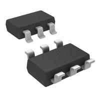
LMP8645HVMK/NOPB National Semiconductor, LMP8645HVMK/NOPB Datasheet - Page 10

LMP8645HVMK/NOPB
Manufacturer Part Number
LMP8645HVMK/NOPB
Description
IC AMP CURRENT SENSE 6TSOT
Manufacturer
National Semiconductor
Datasheet
1.LMP8645MKENOPB.pdf
(16 pages)
Specifications of LMP8645HVMK/NOPB
Amplifier Type
Current Sense
Number Of Circuits
1
Slew Rate
0.6 V/µs
-3db Bandwidth
860kHz
Current - Input Bias
13µA
Voltage - Input Offset
1700µV
Current - Supply
2.2mA
Current - Output / Channel
5mA
Voltage - Supply, Single/dual (±)
2.7 V ~ 12 V
Operating Temperature
-40°C ~ 125°C
Mounting Type
Surface Mount
Package / Case
TSOT-23-6, TSOT-6
Lead Free Status / RoHS Status
Lead free / RoHS Compliant
Output Type
-
Gain Bandwidth Product
-
Other names
LMP8645HVMK
Available stocks
Company
Part Number
Manufacturer
Quantity
Price
www.national.com
Application Information
GENERAL
The LMP8645 and LMP8645HV are single supply high side
current sense amplifiers with variable gain selected through
an external resistor and a common mode voltage Range of
-2V to 42V or -2V to 76V depending on the grade.
The sense voltage is amplified by a user-selected gain and
level shifted from the positive power supply to a ground-re-
ferred output.
THEORY OF OPERATION
As seen from the picture below, the current flowing through
R
high impedance inputs of the amplifier doesn’t conduct this
current and the high open loop gain of the sense amplifier
forces its non-inverting input to the same voltage as the in-
verting input. In this way the voltage drop across R
V
relation:
flows entirely in the external gain resistor developing a voltage
drop equal to
This voltage is buffered and showed at the output with a very
low impedance allowing a very easy interface of the LMP8645
with other ICs (ADC, μC…).
SELECTION OF THE SHUNT RESISTOR
The accuracy of the current measurement strictly depends on
the value of the shunt resistor R
application and it is a compromise between small-signal ac-
curacy and maximum permissible voltage loss in the mea-
surement section. High values of R
at lower currents by minimizing the effects of offset, while low
values of R
most applications, best performance is obtained with an R
V
S
SENSE
G
develops a voltage drop equal to V
= I
I
S
. A current proportional to I
S
′
′
= V
*R
V
S
GAIN
OUT
SENSE
minimize voltage loss in the supply section. For
FIGURE 1. Current monitor
= (R
= (V
/R
IN
SENSE
S
*I
= R
S
)*G, where G = R
/R
S
*I
IN
S
/R
) *R
IN
S
S
. Its value depends on the
GAIN
, where R
according to the following
S
provide better accuracy
= ((R
SENSE
GAIN
S
IN
*I
across R
/R
S
= 1/Gm
)/R
IN
IN
IN
30071603
matches
)*R
S
. The
GAIN
S
10
value that provides a full-scale shunt voltage Range of 100
mV to 200 mV.
SELECTION OF THE GAIN RESISTOR
In the LMP8645 and LMP8645HV the gain is selected through
an external resistor connected to the R
gain resistor R
which is related to the supply voltage and to the common
mode voltage of the input signal. The gain resistor must be
chosen such that the max output voltage does not exceed the
LMP8645 max output voltage rating for a given common
mode voltage.
The following equations explain how to select the gain resistor
for various Range of the input common mode voltage.
The max voltage at the RG pin is given by the following in-
equality V
where Vout_max is the maximum allowable output voltage
according to the Electrical Tables.All the gain resistors
(R
graphical representation in
the combinations (V
lowed.
As a consequence once selected the gain (R
V
quired a Gain of 10, R
Range 10 mV to 100 mV.
In this Range the max voltage at the R
common mode voltage and V
which respect the following inequalities are allowed:
The graphical representation in
tion; all the combinations (V
given V
allowable output voltage according to the Electrical Tables.
SENSE
V
GAIN
RG
) which respect the previous inequality are allowed. The
= V
CM
Range is fixed too. For example if an application re-
V
R
FIGURE 2. Allowed Gains for Range 1
SENSE
G
and supply voltage are allowed.
RG
≤
=V
min (Vout_max; (V
GAIN
Range 1 −2V < V
*R
sense
Range 2 1.8V < V
GAIN
determines the voltage of the output buffer
*R
SENSE
G
*Gm and Vout_max is the maximum
GAIN
will be 50 kΩ and V
, R
Figure 2
where
SENSE
*Gm
SENSE
GAIN
Figure 3
, R
CM
) below the curve are al-
CM
. So all the R
≤
GAIN
helps in the selection; all
CM
- V
≤
min(1.3V; Vout_max)
G
sense
≤
) below the curves for
1.8V
G
pin is related to the
V
helps in the selec-
SENSE
pin. Moreover the
S
-250mV))
GAIN
will be in the
30071604
GAIN
resistors
) the


