LMV301SQ3T2G ON Semiconductor, LMV301SQ3T2G Datasheet
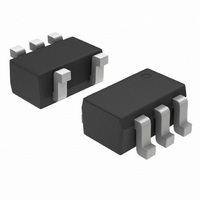
IC OP AMP R-R 1.8V SC70-5

LMV301SQ3T2G

Manufacturer Part Number
LMV301SQ3T2G
Description
IC OP AMP R-R 1.8V SC70-5
Manufacturer
ON Semiconductor
Datasheet

Specifications of LMV301SQ3T2G

Amplifier Type
General Purpose
Number Of Circuits
1
Output Type
Rail-to-Rail
Slew Rate
1 V/µs
Gain Bandwidth Product
1MHz
Current - Input Bias
1nA
Voltage - Input Offset
1700µV
Current - Supply
200µA
Current - Output / Channel
160mA
Voltage - Supply, Single/dual (±)
1.8 V ~ 5 V, ±0.9 V ~ 2.5 V
Operating Temperature
-40°C ~ 85°C
Mounting Type
Surface Mount
Package / Case
SC-70-5, SC-88A, SOT-323-5, SOT-353, 5-TSSOP
Number Of Channels
1
Voltage Gain Db
100 dB
Common Mode Rejection Ratio (min)
50 dB
Input Offset Voltage
9 mV
Operating Supply Voltage
3 V
Supply Current
0.2 mA
Maximum Operating Temperature
+ 85 C
Mounting Style
SMD/SMT
Minimum Operating Temperature
- 40 C
Lead Free Status / RoHS Status
Lead free / RoHS Compliant
-3db Bandwidth
-
Lead Free Status / Rohs Status
 Details

Available stocks

Company
Part Number
Manufacturer
Quantity
Price
Part Number:
LMV301SQ3T2G
Manufacturer:
ON Semiconductor
Quantity:
2 650
Part Number:
LMV301SQ3T2G
Manufacturer:
ADI/亚德诺
Quantity:
20 000
LMV301
Low Bias Current,
1.8V to 5V Single-Supply,
Rail-to-Rail
Operational Amplifier
power supply range from 1.8 V to 5 V and has a quiescent current of
less than 200 mA, maximum, making it ideal for portable
battery−operated applications such as notebook computers, PDA’s and
medical equipment. Low input bias current and high input impedance
make it highly tolerant of high source−impedance signal−sources such
as photodiodes and pH probes. In addition, the LMV301’s excellent
rail−to−rail performance will enhance the signal−to−noise
performance of any application together with an output stage capable
of easily driving a 600 W resistive load and up to 1000 pF capacitive
load. The LMV301 comes in the space saving 5−pin SC−70 package
with an industry−standard pinout, giving it both equivalent function
and similar performance to competitive devices.
Features
Typical Applications
© Semiconductor Components Industries, LLC, 2009
March, 2009 − Rev. 1
The LMV301 CMOS operational amplifier can operate over a
Single Supply Operation (or $V
V
Low Quiescent Current: 185 mA, Max with V
Rail−to−Rail Output Swing
Low Bias Current: 35 pA, max
Space Saving SC70−5 Package
No Output Phase−Reversal when the Inputs are Overdriven
These are Pb−Free Devices
Portable Battery−Powered Instruments
Notebook Computers and PDAs
Cell Phones and Mobile Communication
Digital Cameras
Photodiode Amplifiers
Transducer Amplifiers
Medical Instrumentation
Consumer Products
S
from 1.8 V to 5 V
S
/2)
S
= 1.8 V
1
See detailed ordering and shipping information in the
dimensions section on page 11 of this data sheet.
STYLES 2, 3
SQ SUFFIX
CASE 419A
5
SC70−5
4
+IN
−IN
1 2
V
ORDERING INFORMATION
d
G or G
EE
3
PIN CONNECTION
http://onsemi.com
1
2
3
STYLE 3 PINOUT
= Date Code
= Pb−Free Package
+
MARKING DIAGRAM
Publication Order Number:
AAD
5
4
d
V
OUTPUT
LMV301/D
CC

Related parts for LMV301SQ3T2G

LMV301SQ3T2G Summary of contents

Page 1

LMV301 Low Bias Current, 1. Single-Supply, Rail-to-Rail Operational Amplifier The LMV301 CMOS operational amplifier can operate over a power supply range from 1 and has a quiescent current of less than 200 mA, maximum, ...

Page 2

MAXIMUM RATINGS Symbol V Power Supply (Operating Voltage Range Input Differential Voltage IDR V Input Common Mode Voltage Range ICR Maximum Input Current t Output Short Circuit (Note Maximum Junction Temperature (Operating Range −40°C ...

Page 3

V DC ELECTRICAL CHARACTERISTICS MW / Parameter Input Offset Voltage Input Offset Voltage Average Drift Input Bias Current (Note 2) Common Mode Rejection Ratio Power ...

Page 4

V DC ELECTRICAL CHARACTERISTICS MW / Parameter Input Offset Voltage Input Offset Voltage Average Drift Input Bias Current (Note 2) Common Mode Rejection Ratio Power ...

Page 5

V DC ELECTRICAL CHARACTERISTICS MW / Parameter Input Offset Voltage Input Offset Voltage Average Drift Input Bias Current (Note 2) Common Mode Rejection Ratio Power ...

Page 6

Over −40°C to +85°C 0 Same Gain $1.8 dB (Typ) −10 10k 100k 1M FREQUENCY (Hz) Figure 1. Open Loop Frequency Response ( kW 255C 100 90 ...

Page 7

10k 100k FREQUENCY (Hz) Figure 7. PSRR vs. Frequency ( kW 2.7 V, −PSRR 100 ...

Page 8

out 0.1 0.01 0.001 10 100 1k (Hz) Figure 13. THD+N vs Frequency 0.1 0.09 0.08 0.07 0.06 0.05 0.04 0.03 0.02 Negative Swing 0.01 ...

Page 9

V REFERENCED TO V+ (V) OUT Figure 19. Source Current vs. Output Voltage ...

Page 10

TYPICAL CHARACTERISTICS (T = 25°C and unless otherwise specified V/div 2 ms/div Inverting (G = −1) Figure 25. Step Response − Large Signal http://onsemi.com 10 Input Output ...

Page 11

... LMV301 V V − Figure 28. Comparator with Hysteresis ORDERING INFORMATION Device Pinout Style LMV301SQ3T2G Style 3 †For information on tape and reel specifications, including part orientation and tape sizes, please refer to our Tape and Reel Packaging Specifications Brochure, BRD8011/D. APPLICATIONS V ref ref Hysteresis OH O Given: f ...

Page 12

... Pb−Free strategy and soldering details, please download the ON Semiconductor Soldering and Mounting Techniques Reference Manual, SOLDERRM/D. ON Semiconductor and are registered trademarks of Semiconductor Components Industries, LLC (SCILLC). SCILLC reserves the right to make changes without further notice to any products herein ...

Related keywords