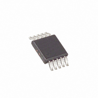
MAX4233AUB+T Maxim Integrated Products, MAX4233AUB+T Datasheet - Page 2

MAX4233AUB+T
Manufacturer Part Number
MAX4233AUB+T
Description
IC OP AMP R-R W/SD 10-UMAX
Manufacturer
Maxim Integrated Products
Datasheet
1.MAX4231EVKIT.pdf
(28 pages)
Specifications of MAX4233AUB+T
Amplifier Type
General Purpose
Number Of Circuits
2
Output Type
Rail-to-Rail
Slew Rate
10 V/µs
Gain Bandwidth Product
10MHz
Current - Input Bias
50pA
Voltage - Input Offset
850µV
Current - Supply
1.2mA
Current - Output / Channel
200mA
Voltage - Supply, Single/dual (±)
2.7 V ~ 5.5 V, ±1.35 V ~ 2.5 V
Operating Temperature
-40°C ~ 125°C
Mounting Type
Surface Mount
Package / Case
10-MSOP, Micro10™, 10-uMAX, 10-uSOP
Number Of Channels
2
Voltage Gain Db
100 dB
Common Mode Rejection Ratio (min)
52 dB
Input Offset Voltage
6 mV
Operating Supply Voltage
3 V, 5 V
Maximum Power Dissipation
444 mW
Maximum Operating Temperature
+ 125 C
Mounting Style
SMD/SMT
Maximum Dual Supply Voltage
+/- 2.5 V
Minimum Operating Temperature
- 40 C
Lead Free Status / RoHS Status
Lead free / RoHS Compliant
-3db Bandwidth
-
Lead Free Status / Rohs Status
Details
High-Output-Drive, 10MHz, 10V/µs,
Rail-to-Rail I/O Op Amps with Shutdown in SC70
ABSOLUTE MAXIMUM RATINGS
Supply Voltage (V
All Other Pins ...................................(V
Output Short-Circuit Duration to V
Continuous Power Dissipation (T
DC ELECTRICAL CHARACTERISTICS
(V
noted.) (Note 2)
Note 1: Package power dissipation should also be observed.
µMAX is a registered trademark of Maxim Integrated Products, Inc.
Stresses beyond those listed under “Absolute Maximum Ratings” may cause permanent damage to the device. These are stress ratings only, and functional
operation of the device at these or any other conditions beyond those indicated in the operational sections of the specifications is not implied. Exposure to
absolute maximum rating conditions for extended periods may affect device reliability.
2
Output Voltage Swing
Operating Supply Voltage Range
Input Offset Voltage
Input Bias Current
Input Offset Current
Input Resistance
Common-Mode Input Voltage
Range
Common-Mode Rejection Ratio
Power-Supply Rejection Ratio
Shutdown Output Impedance
Output Voltage in Shutdown
Large-Signal Voltage Gain
Output Source/Sink Current
Output Voltage
DD
5-Pin SC70 (derate 3.1mW/°C above +70°C) ..............247mW
5-Pin SOT23 (derate 7.1mW/°C above +70°C)............571mW
6-Pin SC70 (derate 3.1mW/°C above +70°C) ..............245mW
6-Pin SOT23 (derate 8.7mW/°C above +70°C)............696mW
6-Pin Thin µDFN (derate 2.1mW/°C above +70°C)...170.2mW
6-Bump UCSP (derate 3.9mW/°C above +70°C) .....308.3mW
8-Pin SOT23 (derate 8.9mW/°C above +70°C)............714mW
_______________________________________________________________________________________
= 2.7V, V
PARAMETER
SS
DD
= 0V, V
to V
SS
CM
) ....................................................6V
= V
DD
A
DD
= +70°C)
or V
/2, V
V
SS
OUT(SHDN)
SYMBOL
CMRR
V
SS
I
PSRR
R
A
OUT
V
V
V
OUT
- 0.3V) to (V
OUT
I
R
OUT
I
OS
VOL
CM
DD
OS
B
(Note 1) ................10s
IN
= (V
DD
Inferred from PSRR test
V
V
Inferred from CMRR test
V
V
V
V
V
< V
R
R
R
V
V
I
I
L
L
CM
CM
SS
DD
SS
DD
DD
SHDN
SHDN
L
L
L
= 10mA
= 30mA
DD
/2), R
= 2kΩ
= 32Ω
= 200Ω
DD
< V
+ 0.20V < V
= 2.7V to 5.5V
= 2.7V, V
= 5V, V
= V
= V
+ 0.3V)
- 0.20V
= 0V (Note 3)
= 0V, R
CM
L
SS
SS
= ∞ connected to (V
to V
to V
< V
IN
IN
V
V
= ±100mV
CONDITIONS
L
DD
DD
DD
DD
DD
OUT
= ±100mV
= 200Ω (Note 3)
= 2.7V
= 5V
Operating Temperature Range .........................-40°C to +125°C
Junction Temperature ......................................................+150°C
Storage Temperature Range .............................-65°C to +150°C
Lead Temperature
Soldering Temperature (reflow) .......................................+260°C
8-Pin µMAX
10-Pin µMAX (derate 5.6mW/°C above +70°C) ..........444mW
10-Bump UCSP (derate 6.1mW/°C above +70°C) .....484mW
14-Pin SO (derate 8.3mW/°C above +70°C) ...............667mW
(excluding 6 and 10 UCSP, soldering, 10s) ................+300°C
R
R
R
V
V
V
V
V
V
DD
OL
DD
OL
DD
OL
L
L
L
= 100kΩ
= 2kΩ
= 200Ω
- V
- V
- V
- V
- V
- V
V
V
V
V
SS
SS
SS
OH
OH
OH
DD
OL
DD
OL
DD
- V
- V
- V
- V
®
/2), V
(derate 4.5mW/°C above +70°C) ..........362mW
SS
SS
OH
OH
SHDN
= V
MIN
V
2.7
52
73
85
74
DD
SS
, T
A
1000
= +25°C, unless otherwise
TYP
0.85
100
360
200
128
112
240
224
400
50
50
70
85
10
68
98
80
80
70
70
8
7
MAX
V
120
500
120
120
200
175
320
300
500
5.5
±6
14
14
DD
UNITS
MΩ
mV
mV
mV
mA
mV
pA
pA
dB
dB
dB
Ω
V
V


