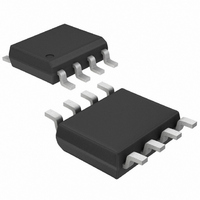
MAX4077ESA+ Maxim Integrated Products, MAX4077ESA+ Datasheet - Page 4

MAX4077ESA+
Manufacturer Part Number
MAX4077ESA+
Description
IC OPAMP OPEN-LOOP R-R OUT 8SOIC
Manufacturer
Maxim Integrated Products
Series
GainAmp™r
Datasheet
1.MAX4076ESA.pdf
(20 pages)
Specifications of MAX4077ESA+
Amplifier Type
General Purpose
Number Of Circuits
2
Output Type
Rail-to-Rail
Slew Rate
0.09 V/µs
Gain Bandwidth Product
230kHz
Current - Input Bias
1pA
Voltage - Input Offset
1200µV
Current - Supply
45µA
Current - Output / Channel
20mA
Voltage - Supply, Single/dual (±)
2.5 V ~ 5.5 V
Operating Temperature
-40°C ~ 70°C
Mounting Type
Surface Mount
Package / Case
8-SOIC (3.9mm Width)
Number Of Channels
2
Voltage Gain Db
117 dB
Common Mode Rejection Ratio (min)
70 dB
Input Offset Voltage
1.2 mV
Operating Supply Voltage
3 V, 5 V
Supply Current
0.09 mA
Maximum Power Dissipation
471 mW
Maximum Operating Temperature
+ 70 C
Mounting Style
SMD/SMT
Minimum Operating Temperature
- 40 C
Lead Free Status / RoHS Status
Lead free / RoHS Compliant
-3db Bandwidth
-
Lead Free Status / Rohs Status
Details
Micropower, SOT23, Rail-to-Rail,
Fixed-Gain, GainAmp/Open-Loop Op Amps
ELECTRICAL CHARACTERISTICS—MAX4076/MAX4077/MAX4078 (continued)
(V
are at V
4
Note 1: All devices are 100% production tested at T
Note 2: Guaranteed by design.
Note 3: The input common-mode range for IN_+ is guaranteed by a functional test. A similar test is done on the IN_- input. See the
Note 4: For A
Note 5: Includes noise from on-chip resistors.
Note 6: The gain accuracy test is performed with the GainAmps in the noninverting configuration. The output voltage swing is limit-
(V
Output Voltage Swing
Gain-Bandwidth Product
Slew Rate
Settling Time (to 0.01%)
Input Voltage Noise Density
Input Noise Current Density
Capacitive Load Stability
Power-Up Time
CC
CC
_______________________________________________________________________________________
-1
-2
-3
-4
-5
-6
4
3
2
1
0
= +2.5V to +5.5V, V
= +5.0V, R
CC
1k
Applications Information section for more information on the input voltage range of the GainAmps.
ed by the input voltage range for certain gains and supply voltage conditions. For situations where the output voltage swing
is limited by the valid input range, the output limits are adjusted accordingly.
SMALL-SIGNAL GAIN vs. FREQUENCY
V
PARAMETER
OUT
= +5V and T
= 100mVp-p
V
= -0.5V/V and A
A
L
V
= 100kΩ to V
= +2.25V/V
10k
FREQUENCY (Hz)
A
= +25°C.) (Note 1)
EE
100k
= 0, V
A
V
CC
V
= +1.25V/V
= -0.25V/V, the output voltage swing may be limited by the input voltage range.
/2, T
IN+
SYMBOL
V
C
OH
GBW
LOAD
A
SR
= V
e
/V
1M
n
= +25°C, unless otherwise noted.)
OL
IN-
= V
R
R
R
V
V
f = 5kHz
f = 5kHz
No sustained oscillations, A
Output settling to 1%
L
L
L
OUT
OUT
-1
-2
-3
-6
-4
-5
CC
0
4
3
2
1
= 10kΩ
= 1MΩ
= 5kΩ
/2, R
1k
A
= 4V step
= 4V step
SMALL-SIGNAL GAIN vs. FREQUENCY
= +25°C. All temperature limits are guaranteed by design.
V
MAX4074/MAX4075
OUT
L
= 100mVp-p
=
∞
A
10k
CONDITIONS
V
to V
FREQUENCY (Hz)
= +4V/V
CC
/2, T
Typical Operating Characteristics
V
V
V
V
V
V
100k
CC
OL
CC
OL
CC
OL
A
V
A
V
- V
- V
- V
- V
- V
- V
= +1V/V
= T
= +2.5V/V
EE
EE
EE
OH
OH
OH
MIN
to T
1M
MAX
, unless otherwise noted. Typical values
-1
-2
-3
-4
-5
-6
4
3
2
1
0
MIN
1k
SMALL-SIGNAL GAIN vs. FREQUENCY
V
OUT
= 100mVp-p
TYP
0.23
0.22
A
100
100
230
110
100
1.1
V
12
90
69
10
10k
7
= +9V/V
FREQUENCY (Hz)
MAX
A
100
100
2.5
2.5
50
50
V
100k
= +5V/V
nV/√Hz
UNITS
fA/√Hz
V/ms
kHz
mV
ms
pF
µs
1M


