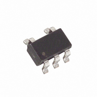
MAX4012EUK+T Maxim Integrated Products, MAX4012EUK+T Datasheet - Page 2

MAX4012EUK+T
Manufacturer Part Number
MAX4012EUK+T
Description
IC OP AMP SNGL SPLY R-R SOT23-5
Manufacturer
Maxim Integrated Products
Datasheet
1.MAX4016ESA.pdf
(17 pages)
Specifications of MAX4012EUK+T
Amplifier Type
General Purpose
Number Of Circuits
1
Output Type
Rail-to-Rail
Slew Rate
600 V/µs
-3db Bandwidth
200MHz
Current - Input Bias
5.4µA
Voltage - Input Offset
4000µV
Current - Supply
5.5mA
Current - Output / Channel
120mA
Voltage - Supply, Single/dual (±)
3.15 V ~ 11 V, ±1.575 V ~ 5.5 V
Operating Temperature
-40°C ~ 85°C
Mounting Type
Surface Mount
Package / Case
SOT-23-5, SC-74A, SOT-25
Number Of Channels
1
Common Mode Rejection Ratio (min)
70 dB
Input Offset Voltage
4 mV
Input Bias Current (max)
5.4 uA
Operating Supply Voltage
5 V, 9 V
Maximum Power Dissipation
571 mW
Maximum Operating Temperature
+ 85 C
Minimum Operating Temperature
- 40 C
Dual Supply Voltage
+/- 3 V, +/- 5 V
Maximum Dual Supply Voltage
+/- 5.5 V
Minimum Dual Supply Voltage
+/- 1.575 V
Mounting Style
SMD/SMT
Shutdown
No
Supply Voltage (max)
11 V
Supply Voltage (min)
3.15 V
Voltage Gain Db
61 dB
Lead Free Status / RoHS Status
Lead free / RoHS Compliant
Gain Bandwidth Product
-
Lead Free Status / Rohs Status
Lead free / RoHS Compliant
ABSOLUTE MAXIMUM RATINGS
Supply Voltage (V
IN_-, IN_+, OUT_, EN_ .....................(V
Output Short-Circuit Duration to V
Continuous Power Dissipation (T
DC ELECTRICAL CHARACTERISTICS
(V
= +25°C.) (Note 1)
Low-Cost, High-Speed, Single-Supply
Op Amps with Rail-to-Rail Outputs
Stresses beyond those listed under “Absolute Maximum Ratings” may cause permanent damage to the device. These are stress ratings only, and functional
operation of the device at these or at any other conditions beyond those indicated in the operational sections of the specifications is not implied. Exposure
to absolute maximum rating conditions for extended periods may affect device reliability.
2
Input Common-Mode
Voltage Range
Input Offset Voltage (Note 2)
Input Offset Voltage
Temperature Coefficient
Input Offset Voltage Matching
Input Bias Current
Input Offset Current
Input Resistance
Common-Mode Rejection Ratio
Open-Loop Gain (Note 2)
Output Voltage Swing
(Note 2)
Output Current
Output Short-Circuit Current
Open-Loop Output Resistance
CC
5-Pin SOT23 (derate 7.1mW/°C above +70°C) ...........571mW
8-Pin SO (derate 5.9mW/°C above +70°C) .................471mW
_______________________________________________________________________________________
= 5V, V
PARAMETER
EE
= 0, EN_ = 5V, R
CC
to V
EE
) ..................................................12V
A
CC
L
= +70°C)
=
SYMBOL
or V
TC
CMRR
R
A
V
EE
I
V
V
I
R
OUT
I
OUT
VOL
OUT
I
OS
SC
CM
OS
VOS
B
IN
to V
EE
- 0.3V) to (V
............. Continuous
CC
/2, V
Guaranteed by CMRR test
Any channels for MAX4016/MAX4018/
MAX4020
(Note 2)
(Note 2)
Differential mode (-1V
Common mode (-0.2V
(V
0.25V
0.5V
1.0V
R
R
R
R
to ground
R
V
Sinking or sourcing
EE
L
L
L
L
L
EE
= 2k
= 150
= 75
= 75
= 20 to V
OUT
- 0.2V)
CC
V
V
V
OUT
OUT
= V
+ 0.3V)
OUT
CC
CC
V
/2, T
4.5V, R
4V, R
CM
CONDITIONS
4.75V, R
or
A
L
(V
= T
= 50
Operating Temperature Range ...........................-40°C to +85°C
Storage Temperature Range .............................-65°C to +150°C
Lead Temperature (soldering, 10s) .................................+300°C
L
CC
T
T
= 150
V
MIN
L
V
V
V
V
V
V
V
V
V
A
A
8-Pin µMAX (derate 4.1mW/°C above +70°C) ............330mW
14-Pin SO (derate 8.3mW/°C above +70°C) ...............667mW
16-Pin QSOP (derate 8.3mW/°C above +70°C) ..........667mW
IN
CC
OL
CC
OL
CC
OL
CC
OL
CM
- 2.25V)
= 2k
= +25°C
= T
to T
- V
- V
- V
- V
- V
- V
- V
- V
MIN
+1V)
+2.75V)
EE
EE
EE
EE
OH
OH
OH
OH
MAX
to T
, unless otherwise noted. Typical values are at T
MAX
V
0.20
MIN
±70
±60
EE
70
52
-
±120
±150
TYP
0.06
0.06
0.30
0.30
0.05
100
5.4
0.1
0.6
0.6
1.1
±1
70
61
59
57
4
8
3
8
V
2.25
CC
MAX
0.50
1.5
1.5
2.0
20
20
20
-
UNITS
µV/°C
M
mA
mA
mV
mV
µA
µA
k
dB
dB
V
V
A


