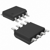
MAX4042ESA+ Maxim Integrated Products, MAX4042ESA+ Datasheet - Page 10

MAX4042ESA+
Manufacturer Part Number
MAX4042ESA+
Description
IC OP AMP R-R DUAL 8-SOIC
Manufacturer
Maxim Integrated Products
Datasheet
1.MAX4040EUKT.pdf
(16 pages)
Specifications of MAX4042ESA+
Amplifier Type
General Purpose
Number Of Circuits
2
Output Type
Rail-to-Rail
Slew Rate
0.04 V/µs
Gain Bandwidth Product
90kHz
Current - Input Bias
2nA
Voltage - Input Offset
200µV
Current - Supply
14µA
Current - Output / Channel
2.5mA
Voltage - Supply, Single/dual (±)
2.4 V ~ 5.5 V, ±1.2 V ~ 2.75 V
Operating Temperature
-40°C ~ 85°C
Mounting Type
Surface Mount
Package / Case
8-SOIC (3.9mm Width)
Number Of Channels
2
Voltage Gain Db
94 dB
Common Mode Rejection Ratio (min)
70 dB
Input Offset Voltage
1.5 mV
Operating Supply Voltage
3 V, 5 V
Supply Current
0.04 mA
Maximum Power Dissipation
471 mW
Maximum Operating Temperature
+ 85 C
Mounting Style
SMD/SMT
Maximum Dual Supply Voltage
+/- 2.75 V
Minimum Operating Temperature
- 40 C
Lead Free Status / RoHS Status
Lead free / RoHS Compliant
-3db Bandwidth
-
Lead Free Status / Rohs Status
Details
The MAX4041 (single) and MAX4043 (dual) feature a
low-power shutdown mode. When the shutdown pin
(SHDN) is pulled low, the supply current drops to 1µA
per amplifier, the amplifier is disabled, and the outputs
enter a high-impedance state. Pulling SHDN high or
leaving it floating enables the amplifier. Take care to
ensure that parasitic leakage current at the SHDN pin
does not inadvertently place the part into shutdown
mode when SHDN is left floating. Figure 4 shows the
output voltage response to a shutdown pulse. The logic
threshold for SHDN is always referred to V
GND). When using dual supplies, pull SHDN to V
enter shutdown mode.
The MAX4040–MAX4044 are fully guaranteed over tem-
perature and supply voltage to drive a maximum resis-
tive load of 25k
be driven in many applications. The rail-to-rail output
stage of the amplifier can be modeled as a current
source when driving the load toward V
rent sink when driving the load toward V
tude of this current source/sink varies with supply
voltage, ambient temperature, and lot-to-lot variations
of the units.
Figures 5a and 5b show the typical current source and
sink capability of the MAX4040–MAX4044 family as a
function of supply voltage and ambient temperature.
The contours on the graph depict the output current
value, based on driving the output voltage to within
50mV, 100mV, and 200mV of either power-supply rail.
Single/Dual/Quad, Low-Cost, SOT23,
Micropower, Rail-to-Rail I/O Op Amps
Figure 3. Rail-to-Rail Input/Output Voltage Range
10
______________________________________________________________________________________
1V/div
1V/div
R
V
f
IN
L
IN
= 100k TIED TO V
= 1kHz
= 4.0V
to V
CC
/ 2, although heavier loads can
200 s/div
Load-Driving Capability
EE
Shutdown Mode
MAX4040-44 fig03
CC
EE
, and as a cur-
CC
. The magni-
OUT
IN
/ 2 (not to
EE
to
Figure 4. Shutdown Enable/Disable Output Voltage
Figure 5a. Output Source Current vs. Temperature
Figure 5b. Output Sink Current vs. Temperature
SHDN
OUT
1200
1000
3000
2500
2000
1500
1000
800
600
400
200
500
0
0
V
R
-60 -40 -20
-60 -40 -20
IN
L
= 100k TIED TO V
= 2V
V
V
V
V
CC
CC
OH
CC
= 5.5V, V
= 2.4V,
= 200mV
= 2.4V, V
V
CC
V
= 5.5V, V
200 s/div
CC
TEMPERATURE (°C)
OL
TEMPERATURE (°C)
OL
= 5.5V, V
0
= 50mV
0
= 200mV
EE
V
OH
CC
20
20
V
V
V
= 200mV
V
CC
= 5.5V, V
CC
OL
CC
CC
= 200mV
= 2.4V, V
= 5.5V, V
= 2.4V, V
= 2.4V, V
40
40
MAX4040-44 fig04
OH
V
V
V
V
CC
OH
60
60
CC
OL
OL
= 100mV
OH
OL
OH
= 2.4V,
= 100mV
= 100mV
= 5.5V,
= 100mV
= 50mV
= 50mV
= 50mV
80
80
5V/div
1V/div
100
100


