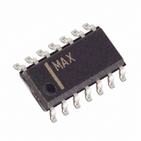
MAX4134ESD Maxim Integrated Products, MAX4134ESD Datasheet - Page 10

MAX4134ESD
Manufacturer Part Number
MAX4134ESD
Description
IC OPAMP QUAD 10MHZ R-RI/O14SOIC
Manufacturer
Maxim Integrated Products
Datasheet
1.MAX4132ESA.pdf
(18 pages)
Specifications of MAX4134ESD
Amplifier Type
General Purpose
Number Of Circuits
4
Output Type
Rail-to-Rail
Slew Rate
4 V/µs
Gain Bandwidth Product
10MHz
Current - Input Bias
50nA
Voltage - Input Offset
350µV
Current - Supply
1mA
Current - Output / Channel
50mA
Voltage - Supply, Single/dual (±)
2.7 V ~ 6.5 V, ±1.35 V ~ 3.25 V
Operating Temperature
-40°C ~ 85°C
Mounting Type
Surface Mount
Package / Case
14-SOIC (3.9mm Width), 14-SOL
Lead Free Status / RoHS Status
Contains lead / RoHS non-compliant
-3db Bandwidth
-
Available stocks
Company
Part Number
Manufacturer
Quantity
Price
Company:
Part Number:
MAX4134ESD+
Manufacturer:
ST
Quantity:
50
Single/Dual/Quad, Wide-Bandwidth, Low-Power,
Single-Supply, Rail-to-Rail I/O Op Amps
Devices in the MAX4130–MAX4134 family of high-
speed amplifiers have rail-to-rail input and output
stages designed for low-voltage, single-supply opera-
tion. The input stage consists of separate NPN and
PNP differential stages that combine to provide an
input common-mode range that extends 0.2V beyond
the supply rails. The PNP stage is active for input volt-
ages close to the negative rail, and the NPN stage is
active for input voltages near the positive rail. The input
offset voltage is typically below 200µV. The switchover
transition region, which occurs near V
extended to minimize the slight degradation in com-
mon-mode rejection ratio caused by the mismatch of
the input pairs. Their low offset voltage, high band-
width, and rail-to-rail common-mode range make these
op amps excellent choices for precision, low-voltage
data-acquisition systems.
Since the input stage switches between the NPN and
PNP pairs, the input bias current changes polarity as
the input voltage passes through the transition region.
Figure 2. Input Protection Circuit
10
______________________________________________________________________________________
Applications Information
Rail-to-Rail Input Stage
1kΩ
1kΩ
CC
/ 2, has been
Reduce the offset error caused by input bias currents
flowing through external source impedances by match-
ing the effective impedance seen by each input
(Figures 1a, 1b). High source impedances, together
with input capacitance, can create a parasitic pole that
produces an underdamped signal response. Reducing
the input impedance or placing a small (2pF to 10pF)
capacitor across the feedback resistor improves
response.
The MAX4130–MAX4134s’ inputs are protected from
large differential input voltages by 1kΩ series resistors
and back-to-back triple diodes across the inputs
(Figure 2). For differential input voltages less than 1.8V,
input resistance is typically 500kΩ. For differential input
voltages greater than 1.8V, input resistance is approxi-
mately 2kΩ. The input bias current is given by the fol-
lowing equation:
I
BIAS
=
V
DIFF
2k
- 1.8V
Ω


