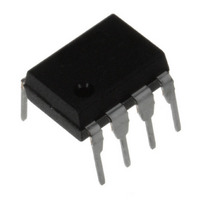
NJM4560D NJR, NJM4560D Datasheet - Page 2

NJM4560D
Manufacturer Part Number
NJM4560D
Description
IC DUAL HIGH GAIN OP AMP 8-DIP
Manufacturer
NJR
Datasheet
1.NJM4560D.pdf
(4 pages)
Specifications of NJM4560D
Amplifier Type
General Purpose
Number Of Circuits
2
Slew Rate
4 V/µs
Gain Bandwidth Product
10MHz
Current - Input Bias
40nA
Voltage - Input Offset
500µV
Current - Supply
4.3mA
Voltage - Supply, Single/dual (±)
±4 V ~ 18 V
Operating Temperature
-40°C ~ 85°C
Mounting Type
Through Hole
Package / Case
8-DIP
Number Of Channels
2
Common Mode Rejection Ratio (min)
70 dB
Input Offset Voltage
6 mV
Input Bias Current (max)
500 nA
Supply Current
5.7 mA
Maximum Power Dissipation
500 mW
Maximum Operating Temperature
+ 85 C
Minimum Operating Temperature
- 40 C
Dual Supply Voltage
+/- 5 V, +/- 9 V, +/- 12 V, +/- 15 V
Maximum Dual Supply Voltage
+/- 18 V
Minimum Dual Supply Voltage
+/- 4 V
Mounting Style
Through Hole
Shutdown
No
Technology
Bipolar
Voltage Gain Db
100 dB
Lead Free Status / RoHS Status
Contains lead / RoHS non-compliant
Output Type
-
Current - Output / Channel
-
-3db Bandwidth
-
Lead Free Status / Rohs Status
Lead free / RoHS Compliant
Available stocks
Company
Part Number
Manufacturer
Quantity
Price
Part Number:
NJM4560D
Manufacturer:
JRC
Quantity:
20 000
Company:
Part Number:
NJM4560DD
Manufacturer:
JRC
Quantity:
5 510
Part Number:
NJM4560DD
Manufacturer:
JRC
Quantity:
20 000
Part Number:
NJM4560DX
Manufacturer:
JRC
Quantity:
20 000
■ ABSOLUTE MAXIMUM RATINGS
( note ) For supply voltage less than ±15V,the absolute maximum input voltage is equal to the supply voltage.
■ ELECTRICAL CHARACTERISTICS
- 2 -
Input Common Mode Voltage Range
Maximum Output Voltage Swing 1
Maximum Output Voltage Swing 2
Common Mode Rejection Ratio
Operating Temperature Range
Supply Voltage Rejection Ratio
Equivalent Input Noise Voltage
Storage Temperature Range
Large Signal Voltage Gain
Gain Bandwidth Product
Differential Input Voltage
Input Offset Voltage
Input Offset Current
Power Dissipation
Input Bias Current
Operating Current
Input Resistance
Supply Voltage
PARAMETER
PARAMETER
Input Voltage
Slew Rate
SYMBOL
SYMBOL
CMR
V
V
V
SVR
V
T
T
R
SR
GB
V
V
V
V
P
A
I
+
I
I
OM1
OM2
CC
IO
ICM
opr
stg
B
/V
ID
IC
IO
IN
NI
D
V
-
RIAA,R
TEST CONDITION
R
L
( DMP8 ) 300
( EMP8 ) 300
≥2kΩ,V
( DIP8 ) 500
( SIP8 ) 800
S
RATINGS
-40~+125
R
R
R
I
=2kΩ,30kHz LPF
-40~+85
O
R
S
S
S
=25mA
± 18
± 30
± 15 ( note )
L
≤
≤
≤
≥2kΩ
10kΩ
10kΩ
10kΩ
O
=±10V
( Ta=25˚C )
UNIT
MIN.
mW
± 12
± 10
± 12
76.5
0.3
˚C
˚C
86
70
V
V
V
-
-
-
-
-
-
-
± 11.5
TYP.
± 14
± 14
100
0.5
4.3
1.2
40
90
90
10
5
5
4
( Ta=25˚C,V
MAX.
200
500
5.7
6
-
-
-
-
-
-
-
-
-
-
Ver.2006-11-17
+
/V
-
=±15V )
µVrms
UNIT
MHz
V/µs
mV
MΩ
mA
nA
nA
dB
dB
dB
V
V
V


