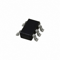
LMV111M5 National Semiconductor, LMV111M5 Datasheet - Page 5

LMV111M5
Manufacturer Part Number
LMV111M5
Description
IC OPAMP W/BIAS NET SOT23-5
Manufacturer
National Semiconductor
Datasheet
1.LMV111M5X.pdf
(9 pages)
Specifications of LMV111M5
Amplifier Type
General Purpose
Number Of Circuits
1
Output Type
Rail-to-Rail
Slew Rate
1 V/µs
Gain Bandwidth Product
1MHz
Current - Supply
130µA
Current - Output / Channel
160mA
Voltage - Supply, Single/dual (±)
2.7 V ~ 5 V
Operating Temperature
-40°C ~ 85°C
Mounting Type
Surface Mount
Package / Case
SOT-23-5, SC-74A, SOT-25
Lead Free Status / RoHS Status
Contains lead / RoHS non-compliant
-3db Bandwidth
-
Current - Input Bias
-
Voltage - Input Offset
-
Other names
LMV111M5TR
Typical Performance Characteristics
25˚C.) (Continued)
Output Voltage Swing vs.
Supply Voltage
Application Section
The LMV111 integrates a rail-to-rail op amp and a V
circuit into one ultra tiny package. With its small footprint and
reduced component count for bias network, it enables the
design of smaller portable electronic products, such as cellu-
lar phones, pagers, PDAs, PCMCIA cards, etc. In addition,
the integration solution minimizes printed circuit board stray
capacitance, and reduces the complexity of circuit design.
The core op amp of this family is National’s LMV321.
1.0 Supply Bypassing
The application circuits in this datasheet do not show the
power supply connections and the associated bypass ca-
pacitors for simplification. When the circuits are built, it is al-
ways required to have bypass capacitors. Ceramic disc ca-
pacitors (0.1µF) or solid tantalum (1µF) with short leads, and
located close to the IC are usually necessary to prevent in-
terstage coupling through the power supply internal imped-
ance. Inadequate bypassing will manifest itself by a low fre-
quency oscillation or by high frequency instabilities.
Sometimes, a 10µF (or larger) capacitor is used to absorb
low frequency variations and a smaller 0.1µF disc is paral-
leled across it to prevent any high frequency feedback
through the power supply lines.
2.0 Input Voltage Range
The input voltage should be within the supply rails. The ESD
protection circuitry at the input of the device includes a diode
between the input pin and the negative supply pin. Driving
the input more than 0.6V (at 25˚C) beyond the negative sup-
ply will turn on the diode and cause signal distortions.
3.0 Capacitive Load Tolerance
The LMV111 can directly drive 200pF capacitive load with
unity gain without oscillation. The unity-gain follower is the
most sensitive configuration to capacitive loading. Direct ca-
pacitive loading reduces the phase margin of amplifiers. The
combination of the amplifier’s output impedance and the ca-
pacitive load induces phase lag. This results in either an un-
derdamped pulse or oscillation. To drive a heavier capacitive
load, a resistive isolation can be used as shown in Figure 1 .
DS101262-22
+
/2 bias
(Unless otherwise specified, V
5
The isolation resistor R
stability by adding more phase margin to the overall system.
The desired performance depends on the value of R
50
evaluation. The bigger the R
stable V
FIGURE 1. Resistive Isolation of a Heavy Capacitive
to 100
OUT
will be.
isolation resistor is recommended for initial
iso
S
and the C
Load
= +5V, single supply, T
iso
resistor value, the more
L
form a pole to increase
www.national.com
A
DS101262-23
=
iso
. A


