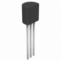
MCP111-475E/TO Microchip Technology, MCP111-475E/TO Datasheet - Page 11

MCP111-475E/TO
Manufacturer Part Number
MCP111-475E/TO
Description
IC VOLT DET 4.63V LOW TO-92
Manufacturer
Microchip Technology
Type
Simple Reset/Power-On Resetr
Specifications of MCP111-475E/TO
Number Of Voltages Monitored
1
Output
Open Drain or Open Collector
Reset
Active Low
Voltage - Threshold
4.63V
Operating Temperature
-40°C ~ 125°C
Mounting Type
Through Hole
Package / Case
TO-92-3 (Standard Body), TO-226
Threshold Voltage
4.63V
No. Of Supervisors / Monitors
1
Supply Voltage Range
1V To 5.5V
Reset Type
Active-Low / Open-Drain
Supply Current
1µA
Delay Time
100µs
Digital Ic Case Style
TO-92
Monitored Voltage
4.63 V
Manual Reset
Not Resettable
Watchdog
No Watchdog
Supply Voltage (max)
5.5 V
Supply Voltage (min)
1 V
Supply Current (typ)
1.75 uA
Maximum Operating Temperature
+ 125 C
Mounting Style
Through Hole
Minimum Operating Temperature
- 40 C
Lead Free Status / RoHS Status
Lead free / RoHS Compliant
Reset Timeout
-
Lead Free Status / Rohs Status
Lead free / RoHS Compliant
4.0
For many of today’s microcontroller applications, care
must be taken to prevent low power conditions that can
cause many different system problems. The most
common causes are brown-out conditions, where the
system supply drops below the operating level momen-
tarily. The second most common cause is when a slowly
decaying power supply causes the microcontroller to
begin executing instructions without sufficient voltage to
sustain SRAM, thus producing indeterminate results.
Figure 4-1 shows a typical application circuit.
FIGURE 4-1:
FIGURE 4-2:
2004 Microchip Technology Inc.
0.1
µF
V
Note 1: R
DD
APPLICATION INFORMATION
MCP11X
due to the open-drain output. Resistor
R
V
V
PU
PU
V
V
DD
OUT
SS
DD
3
is not required with the MCP112.
2
V
may be required with the MCP111
OUT
V
Typical Application Circuit.
V
TRIPMAX
1
V
OUT
TRIPMIN
Operation as Determined by the V
R
PU
1V
Microcontroller
RESET
INPUT
(Active-Low)
PICmicro
< 1 V is outside the
GND
device specifications
V
DD
®
V
TRIPAC
+ V
4.1
The voltage trip point (V
edge of V
be between the minimum trip point (V
maximum trip point (V
this trip point to remove any “jitter” that would occur on
the V
Figure 4-2 shows the state of the V
mined by the V
falling V
V
HYSAC
OUT
TRIP
OUT
will not be driven high until V
DD
pin when the device V
V
and V
DD
voltages. When the V
TRIP
. The actual voltage trip point (V
V
TRIPAC
DD
Operation
HYS
voltage. The V
.
TRIPMAX
MCP111/112
TRIP
) is determined on the falling
). There is a hysteresis on
DD
DD
V
TRIP
TRIPAC
is at the trip point.
DD
voltage is rising, the
specification is for
is at V
DS21889A-page 11
OUT
TRIPMIN
pin as deter-
TRIP
TRIPAC
) and the
+ V
) will
HYS
.


