ADM1069ASTZ Analog Devices Inc, ADM1069ASTZ Datasheet - Page 6
ADM1069ASTZ
Manufacturer Part Number
ADM1069ASTZ
Description
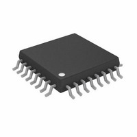
IC SUPERVISOR/SEQUENCER 32-LQFP
Manufacturer
Analog Devices Inc
Type
Sequencerr
Datasheet
1.EVAL-ADM1069LQEBZ.pdf
(32 pages)
Specifications of ADM1069ASTZ
Number Of Voltages Monitored
8
Output
Programmable
Voltage - Threshold
8 Selectable Threshold Combinations
Operating Temperature
-40°C ~ 85°C
Mounting Type
Surface Mount
Package / Case
32-LQFP
For Use With
EVAL-ADM1069LQEBZ - BOARD EVALUATION FOR ADM1069LQ
Lead Free Status / RoHS Status
Lead free / RoHS Compliant
Reset
-
Reset Timeout
-
Available stocks
Company
Part Number
Manufacturer
Quantity
Price
Company:

Part Number:
ADM1069ASTZ
Manufacturer:
AKM
Quantity:
940
Company:
Part Number:
ADM1069ASTZ
Manufacturer:
AD
Quantity:
885
Company:
Part Number:
ADM1069ASTZ
Manufacturer:
Analog Devices Inc
Quantity:
10 000
Part Number:
ADM1069ASTZ
Manufacturer:
ADI/亚德诺
Quantity:
20 000
Company:
Part Number:
ADM1069ASTZ-REEL
Manufacturer:
Analog Devices Inc
Quantity:
10 000
Part Number:
ADM1069ASTZ-REEL
Manufacturer:
ADI/亚德诺
Quantity:
20 000
Company:
Part Number:
ADM1069ASTZ-REEL7
Manufacturer:
Analog Devices Inc
Quantity:
10 000


ADM1069
Parameter
DIGITAL INPUTS (VXx, A0, A1)
SERIAL BUS DIGITAL INPUTS (SDA, SCL)
SERIAL BUS TIMING
SEQUENCING ENGINE TIMING
1
2
At least one of the VH, VPx pins must be ≥ 3.0 V to maintain the device supply on VDDCAP.
Specification is not production tested but is supported by characterization data at initial product release.
Standard (Digital Output) Mode (PDO1 to PDO8)
Three-State Output Leakage Current
Oscillator Frequency
Input High Voltage, V
Input Low Voltage, V
Input High Current, I
Input Low Current, I
Input Capacitance
Programmable Pull-Down Current, I
Input High Voltage, V
Input Low Voltage, V
Output Low Voltage, V
Clock Frequency, f
Bus Free Time, t
Start Setup Time, t
Stop Setup Time, t
Start Hold Time, t
SCL Low Time, t
SCL High Time, t
SCL, SDA Rise Time, t
SCL, SDA Fall Time, t
Data Setup Time, t
Data Hold Time, t
Input Low Current, I
State Change Time
V
V
I
I
R
I
OL
SINK
SOURCE
OH
OL
PULL-UP
2
2
(VPx)
2
BUF
LOW
HIGH
HD;STA
HD;DAT
SCLK
SU;STO
SU;DAT
SU;STA
IL
IL
F
IL
IH
IL
R
IH
IH
OL
2
PULL-DOWN
Min
2.4
V
0
16
90
2.0
−1
2.0
4.7
4.7
4
4
4.7
4
250
5
PU
− 0.3
Rev. B | Page 6 of 32
Typ
20
100
5
20
10
Max
4.5
20
60
29
2
10
110
0.8
1
0.8
0.4
400
1000
300
1
0.50
Unit
V
V
V
V
mA
mA
kΩ
mA
μA
kHz
V
V
μA
μA
pF
μA
V
V
V
kHz
μs
μs
μs
μs
μs
μs
μs
μs
ns
ns
μA
μs
Test Conditions/Comments
V
V
V
I
Maximum sink current per PDOx pin
Maximum total sink for all PDOx pins
Internal pull-up
Current load on any VPx pull-ups, that is, total
source current available through any number of
PDO pull-up switches configured onto any one
VPx pin
V
All on-chip time delays derived from this clock
Maximum V
Maximum V
V
V
VDDCAP = 4.75 V, T
is required
I
V
OL
OUT
PU
PU
PU
PDO
IN
IN
IN
= 20 mA
= 5.5 V
= 0 V
= 0 V
(pull-up to VDDCAP or VPx) = 2.7 V, I
to VPx = 6.0 V, I
≤ 2.7 V, I
= −3.0 mA
= 14.4 V
OH
IN
IN
= 5.5 V
= 5.5 V
= 0.5 mA
OH
A
= 25°C, if known logic state
= 0 mA
OH
= 0.5 mA
Related parts for ADM1069ASTZ
Image
Part Number
Description
Manufacturer
Datasheet
Request
R


Part Number:
Description:
±1.7g Dual-Axis IMEMS Accelerometer Evaluation Board
Manufacturer:
Analog Devices Inc
Datasheet:

Part Number:
Description:
Inertial Sensor Evaluation System
Manufacturer:
Analog Devices Inc
Datasheet:
Part Number:
Description:
Manufacturer:
Analog Devices Inc
Datasheet:
Part Number:
Description:
Manufacturer:
Analog Devices Inc
Datasheet:
Part Number:
Description:
Manufacturer:
Analog Devices Inc
Datasheet:
Part Number:
Description:
Manufacturer:
Analog Devices Inc
Datasheet:
Part Number:
Description:
Manufacturer:
Analog Devices Inc
Datasheet:
Part Number:
Description:
Manufacturer:
Analog Devices Inc
Datasheet:
Part Number:
Description:
Manufacturer:
Analog Devices Inc
Datasheet:
Part Number:
Description:
Manufacturer:
Analog Devices Inc
Datasheet:
Part Number:
Description:
Manufacturer:
Analog Devices Inc
Datasheet:
Part Number:
Description:
Manufacturer:
Analog Devices Inc
Datasheet: