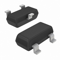
MAX809JTRG ON Semiconductor, MAX809JTRG Datasheet - Page 8

MAX809JTRG
Manufacturer Part Number
MAX809JTRG
Description
IC MPU SUPERVISORY 4.0V SOT23
Manufacturer
ON Semiconductor
Type
Simple Reset/Power-On Resetr
Specifications of MAX809JTRG
Number Of Voltages Monitored
1
Output
Push-Pull, Totem Pole
Reset
Active Low
Reset Timeout
140 ms Minimum
Voltage - Threshold
4V
Operating Temperature
-40°C ~ 105°C
Mounting Type
Surface Mount
Package / Case
SOT-23-3, TO-236-3, Micro3™, SSD3, SST3
Monitored Voltage
1.2 V to 4.9 V
Undervoltage Threshold
3.94 V
Overvoltage Threshold
4.06 V
Manual Reset
No
Watchdog
No
Battery Backup Switching
No
Power-up Reset Delay (typ)
460 ms
Supply Voltage (max)
5.5 V
Supply Voltage (min)
1.2 V
Supply Current (typ)
0.8 uA (Typ)
Mounting Style
SMD/SMT
Maximum Operating Temperature
+ 105 C
Chip Enable Signals
No
Minimum Operating Temperature
- 40 C
Output Type
Active Low or Push-Pull
Power Fail Detection
No
Current, Output
20 mA
Current, Supply
2.5 μA
Package Type
SOT-23
Temperature, Operating, Range
-40 to +105 °C
Voltage, Output, High
4.4 V
Voltage, Output, Low
0.3 V
Voltage, Supply
1.2 to 5.5 V
Number Of Elements
1
Monitored Voltage 1 (typ)
1.2 to 4.9V
Threshold Voltage 1 (max)
4.06V
Watchdog Timer
No
Reset Active Time
460ms
Operating Supply Voltage (min)
1.2V
Operating Supply Voltage (max)
5.5V
Reset Threshold Voltage (max)
4.06V
Reset Threshold Voltage (min)
3.94V
Family Name
MAX809
Operating Temp Range
-40C to 105C
Operating Temperature Classification
Industrial
Mounting
Surface Mount
Pin Count
3
Supply Current
0.0025mA
Lead Free Status / RoHS Status
Lead free / RoHS Compliant
Other names
MAX809JTRGOSTR
Available stocks
Company
Part Number
Manufacturer
Quantity
Price
Part Number:
MAX809JTRG
Manufacturer:
ON/安森美
Quantity:
20 000
Detail Operation Description
supervisory circuits are designed to monitor the power
supplies in digital systems and provide a reset signal to the
processor without any external components. Figure 2 shows
the timing diagram and a typical application below. Initially
consider that input voltage V
than the voltage detector upper threshold (
state for MAX809, or in the low state for MAX 810 devices.
RESET
The
(RESET)
MAX809/810
output voltage (Pin 2) will be in the high
Reset Output
MAX809, NCP803
Reset Output
MAX810
Input Voltage
series
CC
is at a nominal level greater
microprocessor
V
V
V
V
V
0V
V
V
0V
CC
TH+
TH–
CC
TH–
CC
TH–
V TH
Figure 15. Timing Waveforms
). And the
http://onsemi.com
reset
8
If there is an input power interruption and V
significantly deficient, it will fall below the lower detector
threshold (V
in the low state for the MAX809, or in the high state for the
NCP810 devices. After completion of the power
interruption, V
greater than the V
oscillator circuitry and digital counter to count. After the
count of the timeout period, the reset output will revert back
to the original state.
t
RP
TH−
CC
). This event causes the RESET output to be
will rise to its nominal level and become
TH
. This sequence activates the internal
CC
becomes


