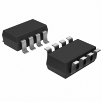
MAX6747KA31+T Maxim Integrated Products, MAX6747KA31+T Datasheet - Page 7

MAX6747KA31+T
Manufacturer Part Number
MAX6747KA31+T
Description
IC RESET MPU W/ADJ RESET SOT23-8
Manufacturer
Maxim Integrated Products
Type
Simple Reset/Power-On Resetr
Datasheet
1.MAX6749KAT.pdf
(14 pages)
Specifications of MAX6747KA31+T
Number Of Voltages Monitored
1
Output
Open Drain or Open Collector
Reset
Active Low
Reset Timeout
Adjustable/Selectable
Voltage - Threshold
3.075V
Operating Temperature
-40°C ~ 125°C
Mounting Type
Surface Mount
Package / Case
SOT-23-8
Monitored Voltage
1.575 V to 5 V
Output Type
Active Low, Open Drain
Manual Reset
Resettable
Watchdog
Watchdog
Battery Backup Switching
No Backup
Supply Voltage (max)
5.5 V
Supply Voltage (min)
1 V
Supply Current (typ)
5 uA
Maximum Power Dissipation
714 mW
Maximum Operating Temperature
+ 125 C
Mounting Style
SMD/SMT
Minimum Operating Temperature
- 40 C
Power Fail Detection
No
Undervoltage Threshold
3.014 V
Overvoltage Threshold
3.137 V
Power-up Reset Delay (typ)
9.487 ms
Lead Free Status / RoHS Status
Lead free / RoHS Compliant
Other names
MAX6747KA31+T
MAX6747KA31+TTR
MAX6747KA31+TTR
The MAX6746–MAX6753 assert a reset signal whenever
the V
threshold. The reset output remains asserted for the
reset timeout period after V
its respective reset threshold. A watchdog timer triggers
a reset pulse whenever a watchdog fault occurs.
The reset and watchdog delays are adjustable with
external capacitors. The MAX6746–MAX6751 contain a
watchdog select input that extends the watchdog time-
out period to 128x.
The MAX6752 and MAX6753 have a sophisticated
watchdog timer that detects when the processor is run-
ning outside an expected window of operation. The
watchdog signals a fault when the input pulses arrive too
early (faster that the selected t
late (slower than the selected t
Figure 1).
The reset output is typically connected to the reset input
of a µP. A µP’s reset input starts or restarts the µP in a
known state. The MAX6746–MAX6753 µP supervisory
circuits provide the reset logic to prevent code-execu-
tion errors during power-up, power-down, and
brownout conditions (see the Typical Operating Circuit ).
RESET changes from high to low whenever the moni-
tored voltage, RESET IN and/or V
reset threshold voltages. Once V
exceeds its respective reset threshold voltage(s),
RESET remains low for the reset timeout period, then
goes high.
Figure 1. MAX6752/MAX6753 Detailed Watchdog Input Timing Relationship
CC
supply voltage or RESET IN falls below its reset
µP Reset Circuits with Capacitor-Adjustable
_______________________________________________________________________________________
Detailed Description
WDI CONDITION 1
WDI CONDITION 2
WDI CONDITION 3
GUARANTEED
TO ASSERT
CC
RESET
WD1
and RESET IN rise above
WD2
*UNDETERMINED STATES MAY OR MAY NOT GENERATE A FAULT CONDITION
RESET IN
timeout period) or too
timeout period) (see
CC
Reset Output
drop below the
Reset/Watchdog Timeout Delay
t
WD1
*UNDETERMINED
and/or V
(MIN) t
WD1
CC
GUARANTEED TO
(MAX)
NOT ASSERT
RESET
RESET is guaranteed to be in the correct logic state for
V
reset logic when V
Ensuring a Valid RESET Output Down to V
The MAX6748–MAX6751 monitor the voltage on RESET IN
using an adjustable reset threshold (V
an external resistor voltage-divider (Figure 2). Use the
following formula to calculate the externally monitored
voltage (V
t
Figure 2. Calculating the Monitored Threshold Voltage
(V
WD2
CC
*UNDETERMINED
MON_TH
(MIN) t
greater than 1V. For applications requiring valid
R1
R2
V
MON_TH
V
WD2
)
MON_TH
MON_TH
(MAX)
GUARANTEED TO
RESET IN
GND
ASSERT
RESET
):
FAST FAULT
NORMAL OPERATION
SLOW FAULT
MAX6748
MAX6749
MAX6750
MAX6751
= V
CC
RESET IN
is less than 1V, see the section
V
CC
RESET IN Threshold
x (R1 + R2) / R2
V
MON_TH
V
CC
= 1.235 x (R1 + R2) / R2
RESET IN
CC
= 0V.
) set with
7


