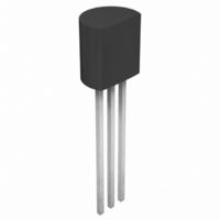
MCP111-450E/TO Microchip Technology, MCP111-450E/TO Datasheet - Page 11

MCP111-450E/TO
Manufacturer Part Number
MCP111-450E/TO
Description
IC VOLT DET 4.38V LOW TO-92
Manufacturer
Microchip Technology
Type
Simple Reset/Power-On Resetr
Specifications of MCP111-450E/TO
Number Of Voltages Monitored
1
Output
Open Drain or Open Collector
Reset
Active Low
Voltage - Threshold
4.38V
Operating Temperature
-40°C ~ 125°C
Mounting Type
Through Hole
Package / Case
TO-92-3 (Standard Body), TO-226
Threshold Voltage
4.38V
No. Of Supervisors / Monitors
1
Supply Voltage Range
1V To 5.5V
Reset Type
Active-Low
Supply Current
1µA
Digital Ic Case Style
TO-92
No. Of Pins
3
Operating
RoHS Compliant
Monitored Voltage
4.38 V
Manual Reset
Not Resettable
Watchdog
No Watchdog
Supply Voltage (max)
5.5 V
Supply Voltage (min)
1 V
Supply Current (typ)
1.75 uA
Maximum Operating Temperature
+ 125 C
Mounting Style
Through Hole
Minimum Operating Temperature
- 40 C
Lead Free Status / RoHS Status
Lead free / RoHS Compliant
Reset Timeout
-
Lead Free Status / Rohs Status
Lead free / RoHS Compliant
4.0
For many of today’s microcontroller applications, care
must be taken to prevent low-power conditions that can
cause many different system problems. The most
common causes are brown-out conditions, where the
system supply drops below the operating level momen-
tarily. The second most common cause is when a slowly
decaying power supply causes the microcontroller to
begin executing instructions without sufficient voltage to
sustain SRAM, thus producing indeterminate results.
Figure 4-1 shows a typical application circuit.
FIGURE 4-1:
FIGURE 4-2:
© 2005 Microchip Technology Inc.
0.1
µF
V
Note 1: R
DD
APPLICATION INFORMATION
MCP11X
due to the open-drain output. Resistor
R
V
V
PU
PU
V
V
DD
OUT
SS
DD
3
is not required with the MCP112.
2
V
may be required with the MCP111
OUT
V
Typical Application Circuit.
V
TRIPMAX
1
V
OUT
TRIPMIN
Operation as Determined by the V
R
(1)
PU
1V
Microcontroller
MCLR
(Reset Input)
PICmicro
< 1 V is outside the
GND
device specifications
V
DD
®
V
TRIPAC
+ V
4.1
The voltage trip point (V
edge of V
be between the minimum trip point (V
maximum trip point (V
this trip point to remove any “jitter” that would occur on
the V
Figure 4-2 shows the state of the V
determined by the V
is for falling V
rising, the V
V
HYSAC
TRIP
TRIP
OUT
+ V
pin when the device V
HYS
V
and V
DD
TRIP
OUT
.
. The actual voltage trip point (V
V
TRIPAC
DD
pin will not be driven high until V
Operation
HYS
voltages. When the V
.
DD
TRIPMAX
MCP111/112
voltage. The V
TRIP
) is determined on the falling
). There is a hysteresis on
DD
V
TRIPAC
is at the trip point.
DS21889D-page 11
TRIP
TRIPMIN
DD
specification
OUT
TRIPAC
voltage is
) and the
pin as
DD
) will
is at


